Publications
See Google scholar Page
- Advancing neural interfaces: a framework for thefabrication and characterization of freestandingmicro-nanodevices
M.J.I. Airaghi Leccardi, B.X.E. Desbiolles, S. Yadav, Y. Yu and D. Sarkar
Microsystems & Nanoengineering, 12, 26 (2026)
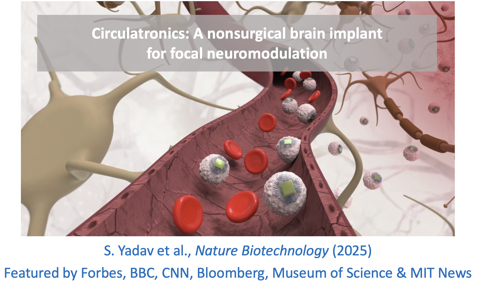
- A nonsurgical brain implant enabled through a cell–electronics hybrid for focal neuromodulation
S. Yadav, R. X. Lee, S. N. Kajale, B. C. Joy, M. Saha, P. Patel, L. Bull, S. Cao, S. Mitragotri, D. C. Bono and D. Sarkar
Nature Biotechnology (2025)
Media coverage by: BBC, Forbes, CNN, Bloomberg, Museum of Science, MIT News
- Low-Frequency Sub-0.5 mm Magnetoelectric Antenna for Wireless Power Harvesting in Injectable Deep-Tissue Implants
Y. Cai, B. C. Joy, B.X.E. Desbiolles, V. Schell, S. Yadav, D. C. Bono and D. Sarkar
IEEE Transactions on Antennas and Propagation, 73, 10 (2025)
Media coverage by: MIT News, Tech Xplore, Electronics For You, Knowridge, Engineeringness
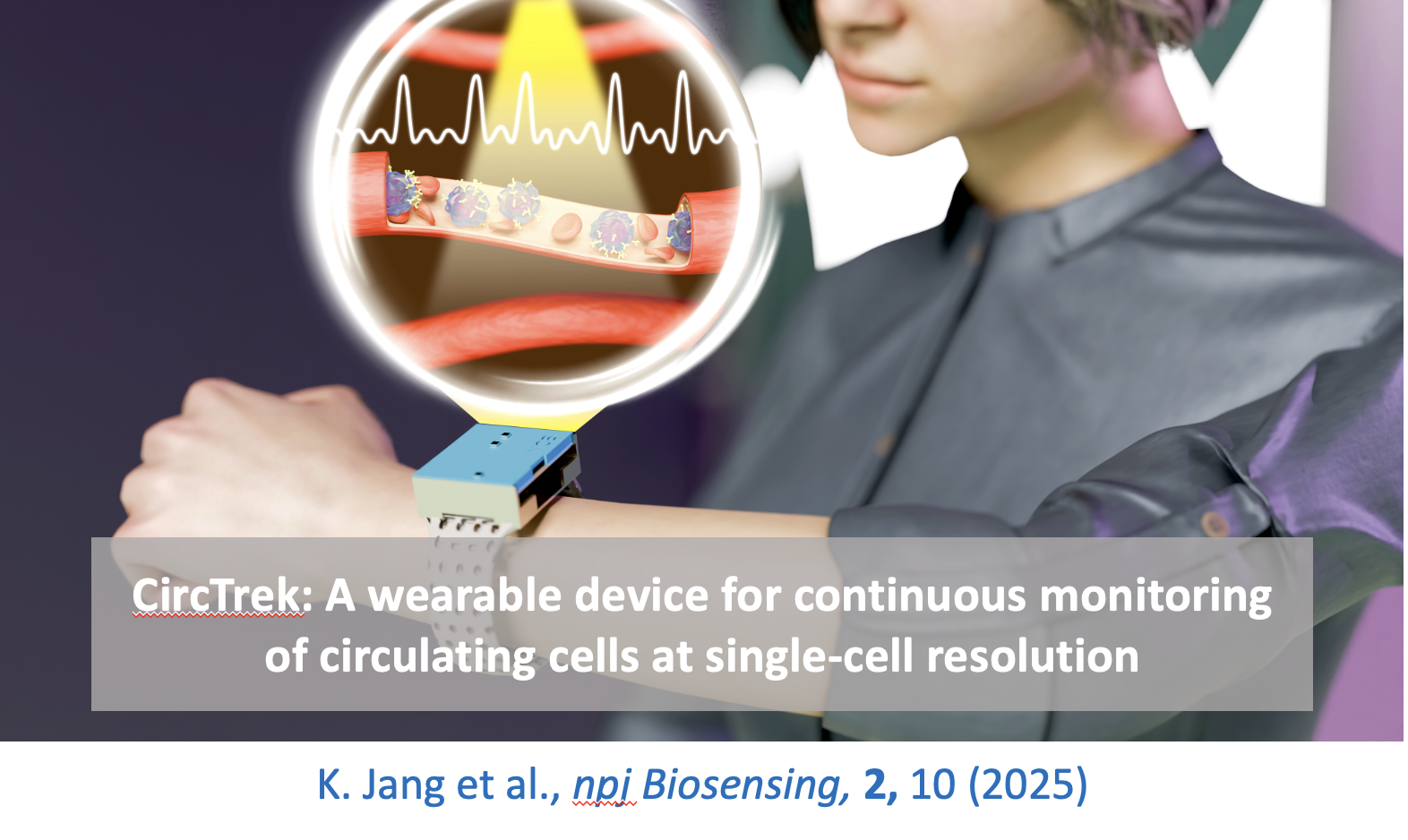
- A wearable device for continuous monitoring of circulating cells at single-cell resolution
K. Jang, S. N. Kajale, B. C. Joy, D. C. Bono, B. Neltner and D. Sarkar
npj Biosensing, 2, 10 (2025)
Media coverage by: MIT News, Medical Economics, AZoSensors, RamaOn Healthcare, START
- Kernel Alignment using Manifold Approximation
M. T. Islam, D. Liu and D. Sarkar
International Conference on Learning Representations (2025)
- Field-free deterministic switching of a van der Waals ferromagnet above room temperature
S.N. Kajale, T. Nguyen, M. Li, and D. Sarkar
APS March Meeting (2025)
- Organic electro-scattering antenna: Wireless and multisite probing of electrical potentials with high spatial resolution
B.X.E. Desbiolles, J. Hanna, R. Ausilio, M.J.I. Airaghi Leccardi, Y. Yu and D. Sarkar
Science Advances, 10, eadr8380 (2024)
Media coverage by: MIT News, Phys.org, EurekAlert!, Tech Explorist, BioCompare
- Energy-Efficient Random Number Generation Using Stochastic Magnetic Tunnel Junctions
N. Alder, S.N. Kajale, M. Tunsiricharoengul, D. Sarkar, and R. Herbrich
NeurIPS Workshop Machine Learning with new Compute Paradigms (2024)
- Light-induced rolling of azobenzene polymer thin films for wrapping subcellular neuronal structures
M.J.I. Airaghi Leccardi, B.X.E. Desbiolles, A.Y. Haddad, B.C. Joy, C. Song and D. Sarkar
Nature Communications Chemistry, 7, 249 (2024)
Media coverage by: MIT News, The Bridge Chronicle, Horizons, MIT Technology Review, EMJ Reviews
- Van der Waals magnetic materials for current-induced control toward spintronic applications
J. Ryu, S. N. Kajale and D. Sarkar
MRS Communications (2024)
- Field-free deterministic switching of all–van der Waals spin-orbit torque system above room temperature
S. N. Kajale, T. Nguyen, N. Tuan Hung, M. Li and D. Sarkar
Science Advances, 10, eadk8669 (2024)
Media coverage by: MIT News, Phys.org, List23, SciTechDaily, Nature Reviews Electrical Engineering
- Current-induced switching of a van der Waals ferromagnet at room temperature
S. N. Kajale, T. Nguyen, C. A. Chao, D. C. Bono, A. Boonkird, M. Li and D. Sarkar
Nature Communications, 15, 1485 (2024)
Media coverage by: MIT News, Storage Newsletter, BNN Breaking, Hoodline, MIT SA+P, Science Daily, myScience, EurekAlert!, Nanotechnology World Association
- Two-dimensional magnetic materials for spintronic applications
S. N. Kajale, J. Hanna, K. Jang and D. Sarkar
Nano Res. 17, 743–762 (2024)
- Deterministic and non-volatile switching of all-van der Waals spin-orbit torque system above room temperature without external magnetic fields
S. N. Kajale, T. Nguyen, M. Li and D. Sarkar
arXiv:2309.04930 [physics.app-ph] (2023)
- Cell Rover: An Intracellular Antenna for Radio Communication in 3D Biological Systems
B. Joy and D. Sarkar
IEEE International Symposium on Antennas and Propagation and USNC-URSI Radio Science Meeting (USNC-URSI), Portland, OR, USA (2023)
- Current-induced deterministic switching of van der Waals ferromagnet at room temperature
S. N. Kajale, T. Nguyen, C. A. Chao, D. C. Bono, A. Boonkird, M. Li and D. Sarkar
arXiv:2306.14355 [physics.app-ph] (2023)
- An Intracellular Antenna For Wireless Probing And Augmentation Of Living Cells
B. Joy and D. Sarkar
American Physical Society Conference, Las Vegas, Nevada, USA (2023)
- An antenna for radio communication in 3D biological systems
B. Joy and D. Sarkar
IEEE AP-S Conference (2023)
- From Green Electronics to Gray Matter and Cyborg Cells
D. Sarkar
IEEE Nanotechnology Magazine, 17, 22-25 (2023)
- Biohybrid Robots: Recent progress, challenges, and perspectives
V. A. Webster-Wood, M. Guix, N. W. Xu, B. Behkam, H. Sato, D. Sarkar, S. Sanchez, M. Shimizu and K. K. Parker
Bioinspiration & Biomimetics, 18, 015001 (2022)
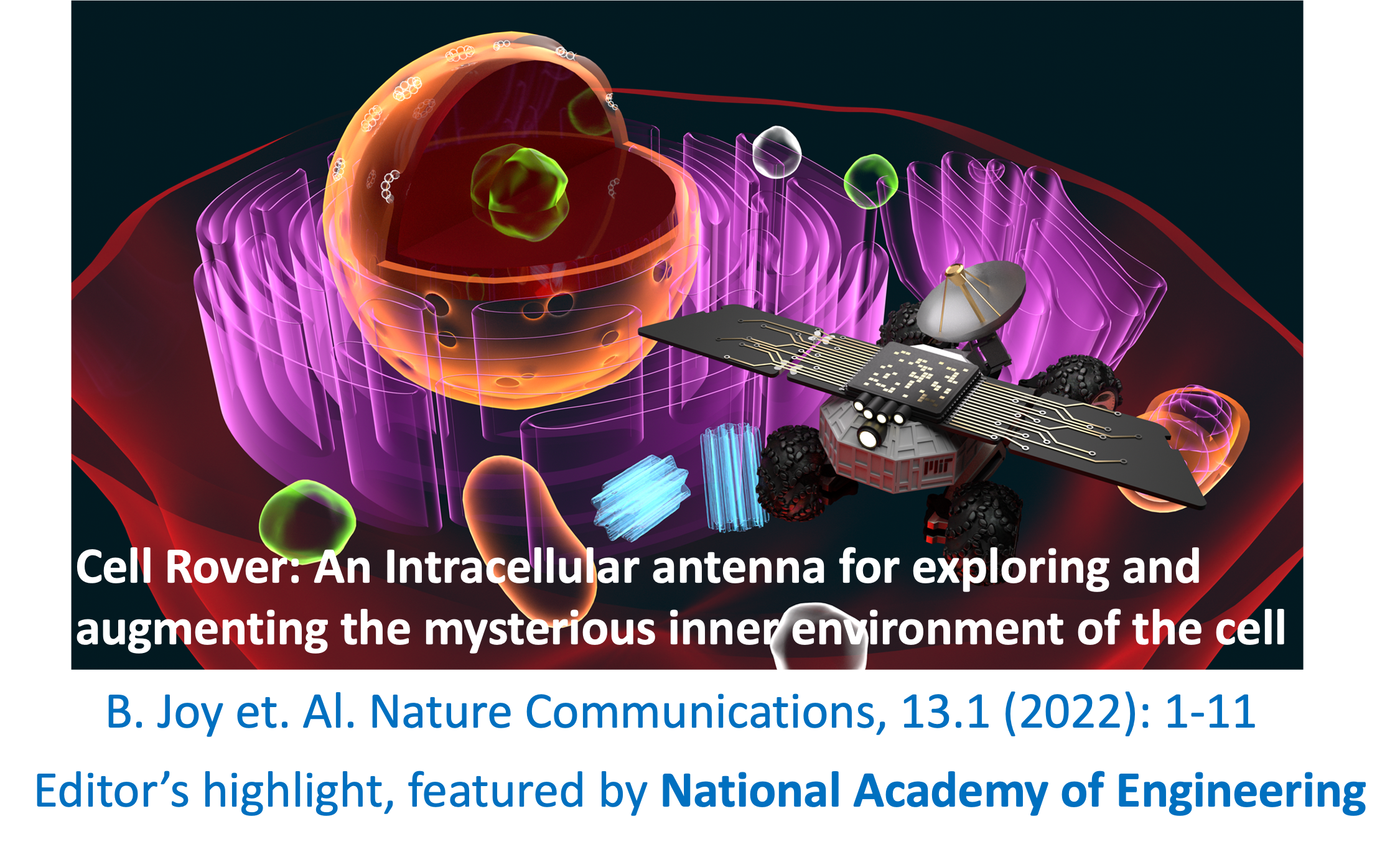
- Cell Rover—a miniaturized magnetostrictive antenna for wireless operation inside living cells
B. Joy, Y. Cai, D. C. Bono and D. Sarkar
Nature Communications, 13, 5210 (2022) ( Editors’ Highlight, featured by the National Academy of Engineering and Scientific American)
Media coverage by: Scientific American,MIT News, Phys.org, Paradigm Research, World Nation, Science Advisory Board, Local Today, Elixir of Science,Azo Sensors, Electronicsforu, Tech Explorist
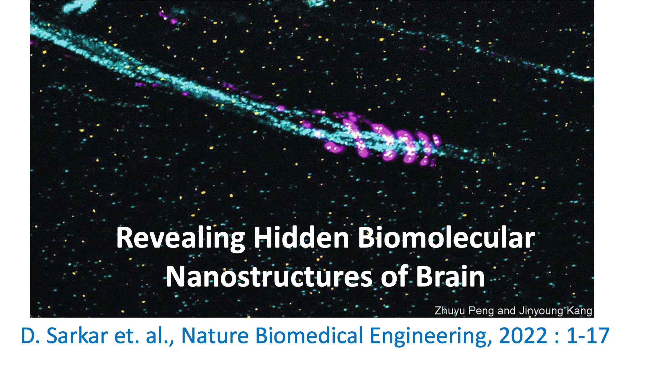
- Revealing nanostructures in brain tissue via protein decrowding by iterative expansion microscopy
D. Sarkar, J. Kang, A. T. Wassie, M. E. Schroeder, Z. Peng, T. B. Tarr, A. Tang, E. D. Niederst, J. Z. Young, H. Su, D. Park, P. Yin, L. Tsai, T. A. Blanpied and E. S. Boyden
Nature Biomedical Engineering, 6, 1057–1073 (2022)
Media coverage by: MIT News, Science Daily, Lab Manager, Science Times, Tech Explorist, Phys.Org,Biotechniques, Genetic Engineering & Biotechnology News
- 2D material-based field-effect-transistors and nano-electro-mechanical systems for sensing applications
S. Kajale*, S. Yadav*, Y. Cai, B. C. Joy and D. Sarkar (* co 1st authors)
iScience, 24, 103513 (2021)
- NEMS Sensors Based on Novel Nanomaterials
S. Yadav, S. Tripathi and D. Sarkar
Advanced MEMS/NEMS Fabrication and Sensors, 133-185 (2021)
- Inhibition of LRRK2 kinase activity promotes anterograde axonal transport and presynaptic targeting of α-synuclein
C. F. Brzozowski, B. A. Hijaz, V. Singh, N. Z. Gcwensa, K. Kelly, E. S. Boyden, A. B. West, D. Sarkar and L. A. Volpicelli-Daley
Acta Neuropathologica Communications, 9, 180 (2021)
- Iterative Direct Expansion Microscopy
D. Sarkar, E. S. Boyden, A. T. Wassie and J. Kang
US Patent App. 16/794, 849 (2020)
- 2D materials for FET based biosensors
D. Sarkar
Fundamentals and Sensing applications of 2D materials, Ed: C.S. Rout, D.J. Late and H. Morgan, Woodhead Publishing Series, Elsevier (2019)
- Computing Systems: From Green Electronics to Gray Matter
D. Sarkar
International Conference on Electrical and Computing Technologies and Applications (ICECTA), Ras Al Khaimah, United Arab Emirates (2019)
Invited Keynote
- Iterative Direct Expansion Microscopy
D. Sarkar, A. Wassie , J. Kang , T. Tarr , A. Tang, T. A. Blanpied and E. S. Boyden
Society for Neuroscience (SFN), Chicago, IL, USA (2019)
- Nanoscale Mapping of the Biomolecular Building blocks of the Brain
D. Sarkar, A. Wassie , J. Kang , T. Tarr , A. Tang, T. A. Blanpied and E. S. Boyden
Biomedical Engineering Society, Philadelphia, PA, USA (2019)
- Tunnel Field Effect Transistors
D. Sarkar
Advanced Nanoelectronics, Ed: M. M. Hussain, Wiley-VCH, 12 (2018)
- Deciphering Nanoscale Biomolecular-Organization of Brain in Health and in Neurological Diseases
D. Sarkar, A. T. Wassie, K. D. Piatkevich and E. S. Boyden
International Conference on Nanoscopy, Bielefeld, NRW, Germany (2018)
Invited
- Glyoxal as an alternative to to PFA in immunostaining and nanoscopy
K. N. Richter, N. H. Revelo, K. J. Seitz, M. S. Helm, D. Sarkar et. al.
European Molecular Biology Organization Journal, 37, 13-159 (2018)
- Mapping the Fundamental Building Blocks of the Brain
D. Sarkar, A. T. Wassie and E. S. Boyden
Lindau Nobel Laureate Meeting (2016)
- 100 fold linear expansion of biological samples for nanoscale imaging
D. Sarkar, A. T. Wassie, A. Payne, K. D. Piatkevich, D. Oran, J.B.Chang and E. S. Boyden
Society for Neuroscience, San Diego, CA, USA (2016)
- Multiplexed neural recording along a single optical fiber via optical reflectometry
S. G. Rodriques, A. H. Marblestone, J. Scholvin, J. Dapello, D. Sarkar, M. Mankin, R. Gao, L. Wood and E. S. Boyden
Journal of Biomedical Optics, 21(5), 057003 (2016)
- Designing Band-to-Band Tunneling Field-Effect Transistors with 2D Semiconductors for Next Generation Low-Power VLSI
W. Cao, J. Jiang, J. Kang, D. Sarkar, W. Liu and K. Banerjee
IEEE International Electron Devices Meeting (IEDM), Washington DC, USA, (2015)
- 2D Semiconductor FETs- Projections and Design for Sub-10 nm VLSI
W. Cao, J. Kang, D. Sarkar, W. Liu and K. Banerjee
IEEE Transactions on Electron Devices, Special Issue to commemorate the 60th anniversary of the IEDM, 62(11), 3459-3469 (2015)
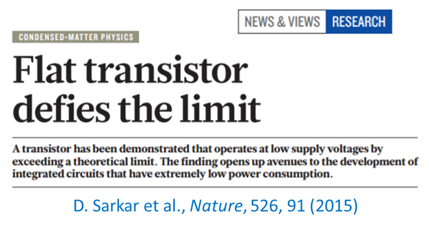
- A Subthermionic Tunnel Field-Effect Transistor with an Atomically Thin Channel
D. Sarkar, X. Xie, W. Liu, W. Cao, J. Kang, Y. Gong, S. Kraemer, P. M. Ajayan and K. Banerjee
Nature, 526, 91–95 (2015)
Media Coverage by Nature, Phy.org,IEEE Spectrum, Science Daily, National Science Foundation, EE Times, National Science Foundation, Physics World, Futuristech, IHS electronics360, nanowrek, HEXUS, EurekAlert, SemiconductorEngineering, Welt der Physik, Inovacao Technologica, New Electronics, Rasberry Projects, Power Systems Design, Simmtester, Compound Semiconductor, Nanotech web, Linkedin, Techxplore, Electronics Lab
- Impact of Contact on the Operation and Performance of Back-Gated Monolayer MoS2 Field-Effect Transistors
W. Liu, D. Sarkar, J. Kang, W. Cao and K. Banerjee
ACS Nano, 9, 8, 7904–7912 (2015)
- Functionalization of Transition Metal Dichalcogenides with Metallic Nanoparticles: Implications for Doping and Gas-Sensing
D. Sarkar, X. Xie, J. Kang, H. Zhang, W. Liu, J. Navarrete, M. Moskovits and K. Banerjee
Nano Letters, 15, 5, 2852–2862 (2015)
- Performance Evaluation and Design Considerations of 2D Semiconductor based FETs for Sub-10 nm VLSI
W. Cao, J. Kang, D. Sarkar, W. Liu and K. Banerjee
IEEE International Electron Devices Meeting (IEDM), San Francisco, CA, USA (2014)
Among 11 Most Significant Papers in IEDM 2014
- Carbon Integrated Electronics
H. Li, Y. Khatami, D. Sarkar, J. Kang, C. Xu, W. Liu and K. Banerjee
Intelligent Integrated Systems: Technologies, Devices and Architectures, Ed: S. Deleonibus, WSPC-Pan Stanford (Singapore) Publishers (2014)
- Graphene Inductors for High-Frequency Applications – Design, Fabrication, Characterization, and Study of Skin Effect
X. Li*, J. Kang*, X. Xie, W. Liu, D. Sarkar, J. Mao and K. Banerjee (*equal contributors)
IEEE International Electron Devices Meeting (IEDM), San Francisco, CA, USA (2014)
- Computational Study of Metal Contacts to Monolayer Transition-Metal Dichalcogenide Semiconductors
J. Kang, W. Liu, D. Sarkar, D. Jena and K. Banerjee
Physical Review X, 4, 3, 031005 (2014)
Media coverage by ECE Department, UCSB
- Low-Frequency Noise in Bilayer MoS2 Transistor
X. Xie, D. Sarkar, W. Liu, J. Kang, O. Marinov, M. J. Deen and K. Banerjee
ACS Nano, 8, 6, 5633-5640 (2014)
- Subthreshold-Swing Physics of Tunnel Field-Effect Transistors
W. Cao, D. Sarkar, Y. Khatami, J. Kang and K. Banerjee
AIP Advances, 4, 067141 (2014)
- Graphene and beyond-graphene 2D crystals for next-generation green electronics
K. Kang, W. Cao, X. Xie, D. Sarkar, W. Liu and K. Banerjee
Proc. SPIE 9083, Micro- and Nanotechnology Sensors, Systems, and Applications VI, 908305 (2014)
- MoS2 Field-Effect Transistor for Next-Generation Label-Free Biosensors
D. Sarkar, W. Liu, X. Xie, A. Anselmo, S. Mitragotri and K. Banerjee
ACS Nano, 8, 4, 3992-4003 (2014)
Media coverage by Phys.org,Medical Design Technology, R&D Magazine, UCSB Current, UCSB Daily Nexus, Med Device Online, AlChE ChEnected, Ceramic Tech Today, Solid Satte Technology, Science Daily, Nanowrek, EurekAlert, Daily Nexus
- Carbon Integrated Electronics
H. Li, Y. Khatami, D. Sarkar, J. Kang, C. Xu, W. Liu and K. Banerjee
in Intelligent Integrated Systems: Technologies, Devices and Architectures. Ed: S. Deleonibus, Pan Stanford Series on Intelligent Nanosystems, 217-274 (2014)
- Controllable and Rapid Synthesis of High-Quality and Large-Area Bernal Stacked Bilayer Graphene using Chemical Vapor Deposition
W. Liu, S. Krämer, D. Sarkar, H. Li, P. M. Ajayan and K. Banerjee
ACS Chemistry of Materials, 26, 2, 907-915 (2014)
Media coverage by Phys.org, Science Daily, Nanowerk, EurekAlert, R&D Magazine,
NanotechWeb,
Clean Technica,
UCSB COE,
- High-Performance Few-Layer-MoS2 Field-Effect-Transistor with Record Low Contact-Resistance
W. Liu, J. Kang, W. Cao, D. Sarkar, Y. Khatami, D. Jena and K. Banerjee
IEEE International Electron Devices Meeting (IEDM), Washington DC, USA (2013)
- 2-Dimensional Tunnel Devices and Circuits on Graphene: Opportunities and Challenges
J. Kang, W. Cao, D. Sarkar, Y. Khatami, W. Liu and K. Banerjee
3rd Berkeley Symposium on Energy Efficient Electronic Systems, Berkeley, CA, USA (2013)
- 2D Electronics: Graphene and Beyond
W. Cao, J. Kang, W. Liu, Y. Khatami, D. Sarkar and K. Banerjee
43rd European Solid-State Device Research Conference (ESSDERC), Bucharest, Romania (2013)
Media coverage by Science Daily, Phys.Org, Nanowerk, National Science Foundation, VyagersIEE UCSBEurekAlert
- Proposal for All-Graphene Monolithic Logic Circuits
J. Kang, D. Sarkar, Y. Khatami and K. Banerjee
Applied Physics Letters, 103, 8, 083113 (2013)
Media coverage by IEEE Spectrum, Extreme Tech, Phys.org, National Science Foundation, Graphene Times,
Physcis News,
Chem Europe,
Graphene Research News,
Printed Electronics World,
AZO Nano,
Bio-Medicine,
The Engineer,
EE Times India
- Graphene and Beyond-Graphene 2D-Crystals for Green Electronics
K. Banerjee, W. Liu, J. Kang, Y. Khatami and D. Sarkar
18th Silicon Nanoelectronics Workshop, Kyoto, Japan (2013)
- Impact-Ionization Field-Effect-Transistor Based Biosensors for Ultra-Sensitive Detection of Biomolecules
D. Sarkar, H. Gossner, W. Hansch and K. Banerjee
Applied Physics Letters, 102, 20, 203110 (2013)
- Role of Metal Contacts in Designing High-Performance Monolayer n-Type WSe2 Field-Effect-Transistors
W. Liu, J. Kang, D. Sarkar, Y. Khatami, D. Jena and K. Banerjee
Nano Letters, 13, 5, 1983-1990 (2013)
Media coverage by Science Daily, Phys.org, Nanowrek, National Science Foundation, EurekAlert
- Tunnel-Field-Effect-Transistor Based Gas-Sensor: Introducing Gas Detection with a Quantum Mechanical Transducer
D. Sarkar, H. Gossner, W. Hansch and K. Banerjee
Applied Physics Letters, 102, 2, 023110 (2013)
- A Computational Study of Metal-Contacts to Beyond-Graphene 2D Semiconductor Materials
J. Kang, D. Sarkar, W. Liu, D. Jena and K. Banerjee
IEEE International Electron Devices Meeting (IEDM), San Francisco, CA, USA (2012)
- Fundamental Limitations of Conventional-FET Biosensors: Quantum-Mechanical-Tunneling to the Rescue
D. Sarkar and K. Banerjee
Device Research Conference (DRC), Penn State University, University Park, PA, USA (2012)
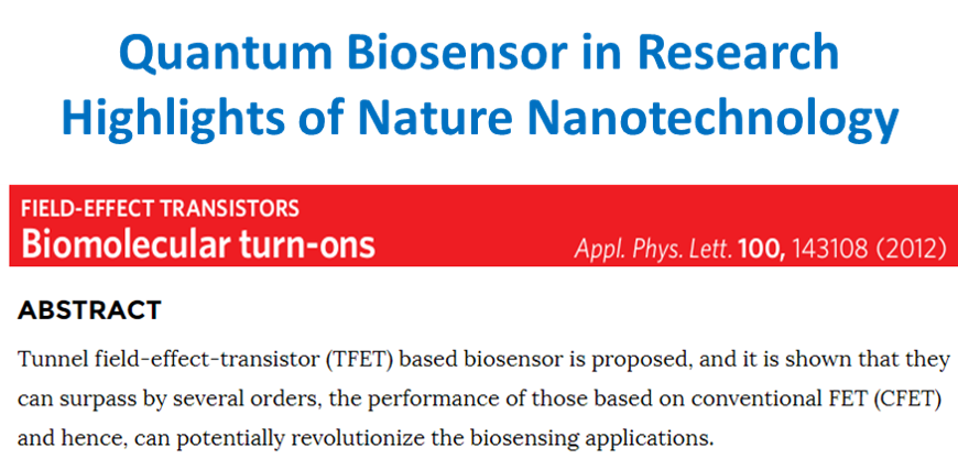
- Proposal for Tunnel-Field-Effect-Transistor as Ultra-Sensitive and Label-Free Biosensors
D. Sarkar and K. Banerjee
Applied Physics Letters, 100, 14, 143108 (2012)
Media coverage by Nature Nanotechnology, EE Times,R&D Magazine, Phys.org, Science Daily, , Medical Design Technology, Nano Werk, NanoTechWeb, EurekAlert, ECE UCSB
- Future of Carbon Nanomaterials as Next-Generation Interconnects and Passives Devices
H. Li, C. Xu, D. Sarkar, Y. Khatami, W. Liu and K. Banerjee
IEEE Electrical Design of Advanced Packaging & Systems (EDAPS) Symposium, Hangzhou, China, (2011)
- Vertically Stacked and Independently Controlled Twin-Gate MOSFETs on a Single Si-Nanowire
X. Li, Z. Chen, N. Shen, D. Sarkar, N. Singh, K. Banerjee, G. Q. Lo and D. L. Kwong
IEEE Electron Device Letters, 32, 11, 1492-1494 (2011)
- Metallic-Nanoparticle Assisted Enhanced Band-to-Band Tunneling Current
D. Sarkar and K. Banerjee
Applied Physics Letters, 99, 13, 133116 (2011)
- High-Frequency Behavior of Graphene-Based Interconnects—Part I: Impedance Modeling
D. Sarkar, C. Xu, H. Li and K. Banerjee
IEEE Transactions on. Electron Devices, 58, 3, 843-852 (2011)
- High-Frequency Behavior of Graphene-Based Interconnects—Part II: Impedance Analysis and Implications for Inductor Design
D. Sarkar, C. Xu, H. Li and K. Banerjee
IEEE Transactions on Electron Devices, 58, 3, 853-859 (2011)
- Electron-hole Duality During Band-to-Band Tunneling Process in Graphene-Nanoribbon Tunnel-FieldEffect Transistors
D. Sarkar, M. Krall and K. Banerjee
Applied Physics Letters, 97, 26, 263109 (2010)
- A Quantitative Inquisition into ESD Sensitivity to Strain in Nanoscale CMOS Protection Devices
D. Sarkar, S. Thijs, D. Linten, C. Russ, H. Gossner and K. Banerjee
IEEE International Electron Devices Meeting (IEDM), San Francisco, CA, USA (2010)
- A Novel Enhanced Electric-Field Impact-Ionization MOS Transistor
D. Sarkar, N. Singh and K. Banerjee
IEEE Electron Device Letters, 31, 11, 1175-1177 (2010)
- Prospects of Carbon Nanomaterials for Next-Generation Green Electronics
K. Banerjee, H. Li, C. Xu, Y. Khatami, H. F. Dadgour, D. Sarkar and W. Liu
IEEE NANO, Kintex, Seoul (2010)
- AC Conductance Modeling and Analysis of Graphene Nanoribbon Interconnects
D. Sarkar, C. Xu, H. Li and K. Banerjee
in Proceedings 13th IEEE International Interconnect Technology Conference (IITC), San Francisco, CA, USA, (2010)
- Experimental Investigation of ESD Performance for Strained Silicon Nano-Devices
D. Sarkar, H. Gossner and K. Banerjee
ESD Forum, Berlin, Germany (2009)
- Modelling of Leakage Current Mechanisms in nanoscale DG MOSFET and its application to low power SRAM design
D. Sarkar, D. Datta and S. Dasgupta
Journal of Computers, 3(2), 37 (2008)
- Spin Selection in Resonant Tunneling Diode using Dilute Magnetic Semiconductors
D. Sarkar
Workshop Recent Adv. Low Dimen. Struc. Dev. (WRA-LDSD), Nottingham, UK (2008)
- Implementation Of A Spintronics Full Adder
D. Sarkar
European Conf. Phys. Magnetism, Poland (2008)
- A Novel Technique for Reduction of Gate Leakage Current Using Double Gate SiGe/Si/SiGe Heterostructure n-Channel Mosfet,
D. Sarkar
Intl. Conf. Low Dimen. Struc. Dev., Columbia (2007)
- Modeling of Leakages in Nanoscale DG MOSFET to Implement Low Power SRAM: a Device/Circuit Co-Design
D. Sarkar, S. Ganguly, D. Datta, A.A.P. Sarab and S. Dasgupta
IEEE Intl. Conf. VLSI Design, Bangalore, India (2007)
- A New Design Architecture of Novel Nanoscale Device to Reduce Leakage Currents
D. Datta, A. A. Sarab, S. Ganguly, D. Sarkar and S. Dasgupta
IEEE Silicon Nanotech. Workshop, HI, USA (2006)