MIDI Controlled Sample-Based Synthesizer
Amir Hirsch and Andrew Leiserson
Overview | Communication | Master Control Unit | Sound Generation Unit | Mixer
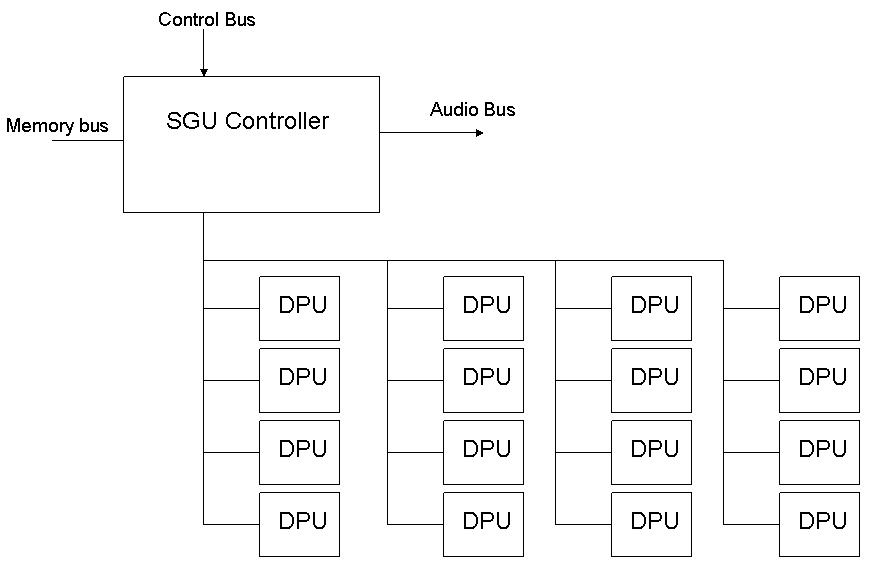
The sound generation unit (SGU) is responsible for generating all of the audio output. It contains a controller and an array of Data Processing Units (DPU). The controller receives commands from the Master Control Unit and distributes the computation of the audio output between the various DPU's by coordinating the functions of each DPU. The SGU also has a subunit which accesses the sample RAM in order to get the samples for interpolation.The protocol used on the DPU bus is similar to that of the Master Control Bus. The SGU Controller indicates in the first byte which DPU it is talking to and the function for the DPU to perform. Bytes are then sent to the DPU containing the data that needs to be processed.
A block diagram of the SGU is below:
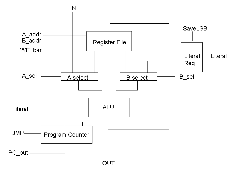
The DPU's each contain a datapath and a ROM. The datapath consists of a 24-bit ALU, an 11-bit Program Counter and a 32-address deep by 24-bit wide dual-port Register File. The register file can output two addresses, A and B, and when write-enable bar of the register file is low, the register file will write the output of the ALU to register A. The ALU Functions are as follows:
0h = SET_RADIX_B (used to set the radix point for multiplication)
1h = OUTPUT A
2h = OUTPUT B
3h = ADD A+B
4h = SUB A-B
5h = MULT A*B
6h = SHIFT A >> B
7h = COMPEQ A == B
8h = COMPLT A < B
9h = COMPGT A > B
Ah = COMPNE A != B
Bh = BIT_WISE_AND A & B
Ch = BIT_WISE_INVERT ~A
Dh = XOR A XOR B
Eh = OR A || B
Fh = CLIP (if A > B then B, if A < -B then -B)
The ROM contains each of the functions the DPU can perform in as a listing of 28-bit bytecodes. The Program Counter of the datapath jumps to the correct function in ROM if the SGU controller indicates a function call is intended for the particular DPU. The format for the byte code is as follows:
ALU_Function[3:0]
Output_Enable
Write_Enable_bar
JMP
SaveLSB (saves the Literal as the bottom 12 bits for use the next cycle)
A_sel[1:0] (00 = Reg_A, 01={IN,0000} 10={00,IN,00} 11={0000,IN})
A_addr[4:0]
B_sel
B_addr[4:0] / Literal[11:7] (MSB of literal indicates if a JMP is conditional)
Literal[6:0]
All of the functions of the DPU were written in an assembly language for which Amir wrote an assembler in Scheme (see the Appendix). A schematic of the datapath is below: