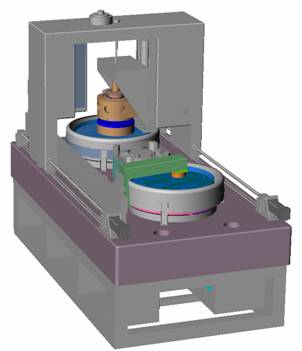
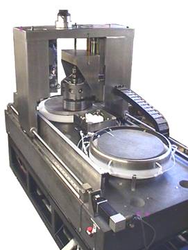
| 1. Axiomatic Design of CMP Machine [top]
Axiomatic design is investigated as a design methodology for large or complex system design. Particular considerations of system design are described and the suitability of axiomatic design for such considerations is discussed. Then, tools to enable successful application of axiomatic design to systems are developed. A design of a machine tool system for polishing silicon wafers using chemical mechanical polishing (CMP) is presented. The CMP system architecture is decomposed from top level requirements using the principles of axiomatic design, and the theorems developed. The CMP system was designed and fabricated by this research group, and has demonstrated excellent capability to remove material from the surface of a wafer while maintained an increased control of the removal.
|
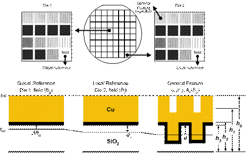
| 2. Process Analysis for Cu CMP [top]
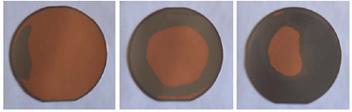
This research establishes a theoretical framework to relate the process parameters to the different wafer/pad contact modes to study the behavior of wafer-scale polishing. Several models of polishing - microcutting, brittle fracture, surface melting and burnishing - are reviewed. Blanket wafers coated with a wide range of materials are polished to verify the models. Plastic deformation is identified as the dominant mechanism of material removal in fine abrasive polishing. Additionally, contact mechanics models, which relate the pressure distribution to the pattern geometry and pad elastic properties, explain the die-scale variation of material removal rate (MRR) on pattern geometry. Experiments study the effects of pattern geometry on the rates of pattern planarization, oxide overpolishing and Cu dishing.
|
| 3. Modeling Dielectric Erosion and Cu Dishing in Single- and
Multi-Step Cu CMP [top]
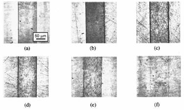
A formidable challenge in the present multi-step Cu CMP process, employed in the ultra-large-scale integration (ULSI) technology, is the control of wafer surface non-uniformity, which primarily is due to dielectric erosion and Cu dishing. In contrast with the earlier experimental and semi-theoretical investigations, a systematic way of characterizing and modeling dielectric erosion in both single- and multi-step Cu CMP processes is presented. Wafer- and die-level erosion are defined, and the plausible causes of erosion at each level are identified in terms of several geometric and physical parameters. The local pressure distribution is estimated at each polishing stage based on the evolving pattern geometry and pad deformation. The single-step model is adapted for the multi-step polishing process, with multiple sets of slurry selectivities, applied pressure, and relative velocity in each step. Based on the developed multi-step erosion model, the physical significance of each model parameter on dielectric erosion is determined, and the optimal polishing practices for minimizing erosion in both multi-step and single-step polishing are suggested.
|
| 4. Slurry-Switching Point and
End-Point Detection in Cu CMP [top] A novel in situ detection technique, based on the change of the reflectance of the patterned surface at different polishing stages, is developed to detect the process end-point and slurry-switching point in multi-step Cu CMP. Models that employ light scattering theory and statistical treatment correlate the sampled reflectance with the surface topography and Cu area fraction for detecting the process regime and end-point. Developed multi-step dielectric erosion and Cu dishing models are applied to minimize resulting Cu thinning.
|