

The Sawin Squad
Research
| |
|
||||||||
The Sawin Squad
|
|||||||||
Research |
|||||||||
Approximately 40% of the steps in the fabrication of microelectronics use plasma processes. Applications in micro-machining, flat panel displays, surface modification, cleaning, sterilization, sputter coating, and many other areas are rapidly growing based largely on technological developments made for the processing of microelectronics. Fundamental understanding of plasma processes is now sufficient that plasma models are emerging as tools for the developing new plasma equipment and processes, as well as, the diagnosing process difficulties. In addition, plasma diagnostics are now being implemented as process monitors, end point detectors, and process controllers to improve processing flexibility and reliability.
The fabrication of integrated circuits involves a stepwise manufacturing process which is simplistically illustrated in the figures below a f. The film to be patterned is coated with a light sensitive polymer material knows as photoresist. The photoresist is exposed to radiation through a mask. Exposed areas of the resist undergo a change in structure, and upon development, wash away (for a positive tone resist). The remaining patterned resist on the wafer acts as a mask, protecting the underlying film material. This process is know as lithography. After patterning, the areas unprotected by photoresist are etched, typically via a plasma etching process. Following the etch, the remaining resist is stripped, leaving features remaining in the film. These steps (film deposition, lithography, and etch) are repeated over and over, with different imaging masks, in order to build up the many layers that make up the completed integrated circuit.
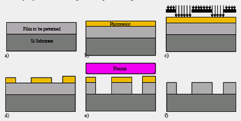
a) Film to be patterned is deposited on a substrate. b) The film is coated with a light sensitive polymer known as photoresist. c) The resist is exposed through a mask consisting of transparent and opaque regions defining the desired circuit features. d) After exposure, the resist is developed, leaving portions of the film masked by undissolved resist. e) The film is etched in a plasma process, leaving the areas protected by resist. f) The remaining resist is stripped, leaving a patterned film. These processes are then repeated over and over to build up the circuit layers.
Feedback control and diagnostics of plasma processes in a split coil inductively coupled plasma reactor using Full Wafer Interferometry and Optical Emission Spectroscopy. Feedback control of etching rate and uniformity on polysilicon etches has been demonstrated on a Lam TCP etcher. Currently, control of Aspect Ratio Dependent Etching (ARDE) which is also known as RIE lag is being developed.
Optical emission spectra reduction by principal component analysis and other techniques for feedback control and endpoint detection.
Oxide reactive ion etching: measurement of surface kinetics and development of novel gases. The
kinetics of oxide etching needed for profile evolution modeling are being measured using the following:
-Mass spectroscopy to measure the ion flux
-UV absorption and Optical Emission analysis to measure the neutral flux
-Quartz crystal microbalance to measure the etching/deposition rate as a function of ion energy and
impingement angle
Ion-induced surface kinetics of polysilicon, oxide, and photoresist etching using beam scattering. Using combinations of up to three beams of F, CF2, F2, Cl2, Cl, Ar+, Cl+, and SiCl2 the surface kinetics of polysilicon, oxide, and photoresist are being measured as a function of ion energy, ion impingement angle, and beam fluxes. In addition, the surface is analyzed using XPS and Laser-Induced Desorption Mass Spectroscopy to determine the elemental composition during and after etching. Kinetic models based on mass balances have been constructed for incorporation in the profiles simulator.
Profile evolution modeling of etching and deposition processes based on Monte Carlo computation of the
fluxes within a surface feature. This simulator includes the following physics and chemistry:
-Ion transport and specular/diffuse scattering from feature surfaces;
-Neutral transport with diffuse scattering;
-Recombination at surfaces as a function of surface composition;
-Deposition of plasma species;
-Re-deposition of etching products
-Surface kinetics based on elemental mass balances;
-Profile advancement by cell removal.
Polysilicon etching surface kinetics and profile evolution modeling in a Lam TCP. Profiles of Cl2 and HBr+Cl2 are being developed using the Monte Carlo profile simulator described above.
Pulsed plasma and pyrolytic deposition of fluorocarbon films for low-k dielectrics.
Plasma abatement of perfluorocompounds.
Ion-induced deposition of metals from organometallics. By adding H atoms, 99% pure Cu can be deposited. HF vapor dry wafer cleaning for in situ oxide and alkali metal removal. Ultraviolet-Chlorine cleaning of Cu, Ni, and Fe. Pyrolytic beam cleaning of Cu, Ni, and Fe.Integrated etch-ash-dry clean-deposition processing for contacts and vias.
Shown in the figure below is an integrated cluster processing system that is in Herb Sawin's lab at MIT. It consists 10process and analytical chambers attached to an ultrahigh vacuum transfer system. The transfer system is maintained at pressures of ~ 10-8 Torr. The samples or wafers are loaded using a load-lock chamber and then transferred to/or between any process chambers without exposure to air. X-ray Photoelectron Spectroscopy (XPS), Auger Electron Spectroscopy (AES), spectroscopic ellipsometer can be used to analyze the wafer surface before, during, and after processing.

This VAST (VAcuum Sample Transfer) tube processes 4" wafers
Presently mounted on the transfer systems are the following:
- X-Ray Photoelectron Spectroscopy (XPS)/AES analytical chamber with angularly
resolution capability for wafer elemental and chemical bonding analysis--using angular resolution,
the composition of tops,
sidewalls, and bottom of patterned features can be deconvoluted;
- Inductively coupled plasma etchers (ICP)--These have a full wafer interferometer
(FWI) for etching rate and uniformity analysis, a mass spectrometer (MS) extraction
orifice for ion composition analysis, and a quartz crystal microbalance (QCM)
sampling orifice for surface kinetic measurements;
- Down-stream plasma asher;
- HF vapor cleaning chamber--it has a spectroscopic ellipsometer allowing in situ
analysis of the etching rate and film properties;
- Sputter deposition chamber;
- Multibeam scattering chamber for ion-induced etching reaction analysis;
- Scanning tunneling microscopy (STM) - Atomic force microscopy (AFM) chamber
for nanoscale measurements;
- Pulsed plasma and pyrolytic CVD chamber of perflourocarbon film deposition for
low-k dielectrics.