
RESEARCH
Research Overview
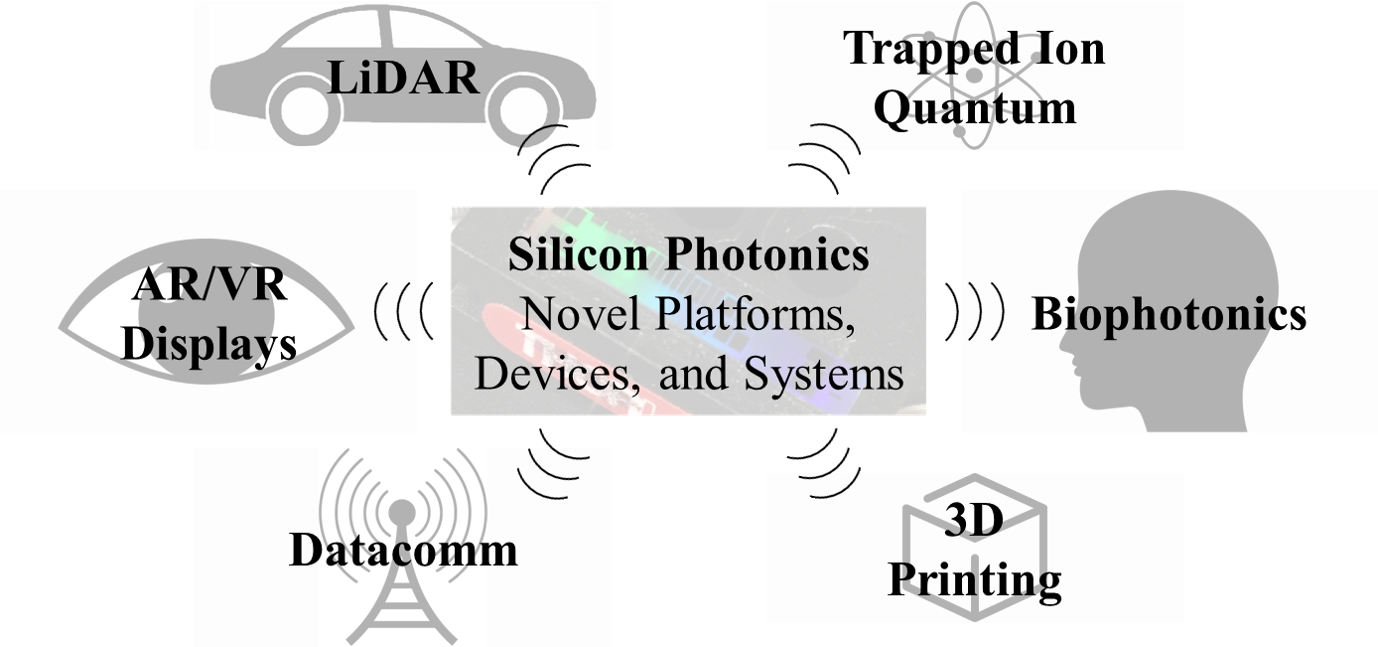
By enabling the integration of millions of micro-scale optical components on compact millimeter-scale computer chips, the field of silicon photonics is positioned to enable next-generation optical technologies that facilitate revolutionary advances for numerous fields spanning science and engineering. In the MIT Photonics and Electronics Research Group (PERG), we are developing novel silicon-photonics-based platforms, devices, and systems that enable innovative solutions to high-impact problems in areas including augmented-reality displays, LiDAR sensing for autonomous vehicles, free-space optical communications, optical trapping for biophotonics, 3D printing, and trapped-ion quantum engineering. See below for descriptions of several recent projects.
|
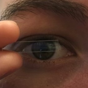
Silicon Photonics for Holographic AR DisplaysAugmented-reality head-mounted displays that display information directly in the user’s field of view have many wide-reaching applications in defense, medicine, engineering, gaming, etc. However, current commercial head-mounted displays are bulky, heavy, and indiscreet. Moreover, these current displays are not capable of producing holographic images with full depth cues; this lack of depth information results in users experiencing eyestrain and headaches that limit long-term and wide-spread use of these displays (an effect known as the vergence-accommodation conflict). To address these limitations, we are developing a novel integrated-photonics-based augmented-reality display that consists of a single discreet transparent chip that sits directly in front of the user's eye and projects visible-light 3D holograms that only the user can see. It enables a highly-discreet and fully-holographic solution for the next generation of AR displays. |

|
Silicon Photonics for Chip-Based 3D PrintersImagine if it were possible to create 3D objects in the palm of your hand within seconds using only a single chip. Although 3D printing has revolutionized the way we create, current 3D printers rely on large and complex mechanical systems to enable layer-by-layer addition of material. This limits the print speed, resolution, portability, form factor, and material complexity. Although there have been efforts in developing photocuring-based 3D printers that utilize light to transform matter from liquid resins to solid objects using advanced methods, they remain reliant on bulky and complex mechanical systems. To address these limitations, we are developing the first chip-based 3D printer that consists of only a single millimeter-scale chip without any moving parts that emits reconfigurable holograms up into a simple stationary resin well to enable non-mechanical 3D printing. It presents a highly-compact, portable, and low-cost solution for the next generation of 3D printers. |
|
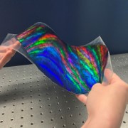
Silicon Photonics with Transparent and Flexible PlatformsSilicon-photonics demonstrations have primarily focused on wafer-scale fabrication processes on silicon substrates that result in opaque and rigid photonic wafers and chips. Nevertheless, there are many application areas that would benefit from either transparent silicon-photonics chips (such as near-eye displays) or mechanically-flexible silicon-photonics chips (such as wearable healthcare monitors). To enable the field of silicon photonics to further advance into these new application areas, we are developing the first transparent and the first mechanically-flexible 300-mm-wafer-scale silicon-photonics platforms in collaboration with our foundry partners. |
|
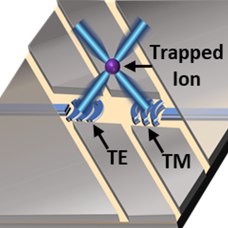
Silicon Photonics for Trapped-Ion Quantum SystemsQuantum computing has emerged as an important tool for solving critical problems that are nearly or completely unsolvable by traditional computers. One of the leading quantum-computing technologies is trapped ions due to their high accuracy and stability (with long coherence times and strong ion-ion interactions). However, most current trapped-ion systems rely on complex free-space optical setups for ion control, whose large size and susceptibility to vibrations hinder scaling to large qubit numbers. Although recent work has shown that utilizing integrated photonic devices for optical interfacing to ions significantly increases stability and potential for scalability, these prior demonstrations have been limited to basic operations using light of only a single linear polarization, limiting the functionality. To address these limitations, we are developing novel polarization-diverse integrated-photonics-based devices and systems to enable advanced functionality for trapped-ion quantum systems. |
|
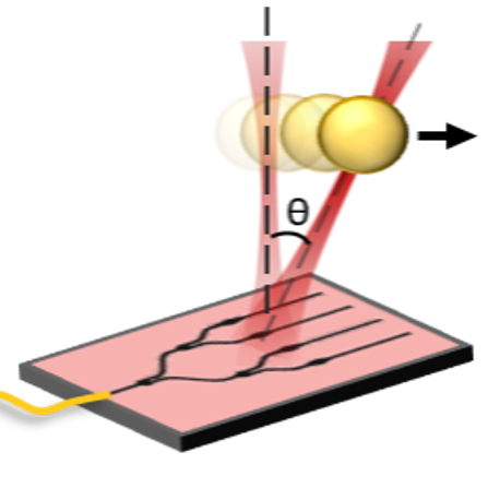
Silicon Photonics for Optical Tweezers for BiophotonicsOptical tweezers enable noncontact manipulation and monitoring of microscale particles using optical forces. As a result, they have become important tools in biology, producing impactful results ranging from understanding DNA mechanics to cell sorting. However, standard optical tweezers utilize free-space bulk-optics setups, whose large form factors, complexity, and limited scaling potential have hindered their utility outside the laboratory and for high-throughput experiments. Although recent work has turned towards integrated optical tweezers for improved form factors, complexity, and scalability, these demonstrations have been fundamentally limited to trapping directly above the surface of the chip, making them incompatible with practical biological experiments and for in-vivo applications. To address these limitations, we are developing the first optical tweezers based on integrated optical phased arrays that increase the standoff distance of integrated optical tweezers by two orders of magnitude compared to prior work and are using this system to demonstrate the first cell experiments performed using single-beam integrated optical tweezers. |
|
Silicon Photonics for Solid-State LiDAR SensorsLight detection and ranging (LiDAR) has emerged as a vital and widely-used sensing technology for autonomous systems, such as autonomous vehicles, since it enables 3D mapping with higher resolution than traditional RADAR. However, current commercial LiDAR systems utilize mechanical beam-steering mechanisms that decrease reliability, increase production cost, and reduce detection range. To address these limitations, we are developing novel solid-state LiDAR systems based on integrated optical phased arrays that enable non-mechanical beam steering and coherent detection schemes for a low-cost, compact, durable, long-range, and high-speed solution for next-generation LiDAR sensors for autonomous systems. |