Ultra-Scalable and Energy-Efficient Nanoelectronics
Artificial intelligence has revolutionized our world and has potential to alter the course of humanity. However, traditional computers are energy inefficient and create a bottleneck for implementation of future intelligent systems. In the past, the growth in computing capabilities of electronics has been sustained by scaling both the dimensions as well as power-supply voltage of the Field-Effect-Transistors (FETs), that form the building blocks of the integrated circuits. However, as the scaling roadmap enters the sub-5 nm regime, today’s transistor reaches its physical limits in dimensional scalability and can no longer offer effective electrostatics, leading to exponential increase in static leakage power. In addition, the power supply voltage, which is the most effective way for lowering the dynamic power, can no longer be scaled effectively as in earlier technology generations. The voltage in-scalability has fundamental roots in the thermal distribution of carriers, which limits the steepness of turn-on characteristics or subthreshold swing of conventional FETs. These dimensional and voltage scalability issues, lead to exponential increase in power-density and has ushered in the dead end of the glorious growth episode of 'Information Society'. Moreover, the fundamental nature of the problem suggests the inability of evolutionary solutions to address this growing energy crisis and demands radically new innovations on multiple fronts.
Our research involves a holistic approach towards solving this energy crisis, starting from exploration of beyond-Silicon nanomaterial technology, to in-depth understanding of the physics of fundamentally different device-working mechanisms ( such as Quantum devices, Spintronics, Neuromorphic ) and finally, experimental demonstration of novel, highly energy-efficient and scalable electronic devices. Such electronic devices can lead to "Green" Information Technology and sustain the growth of Artificial Intelligence
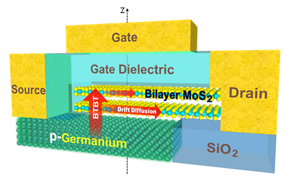
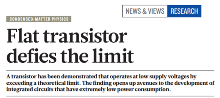
We invented the world’s thinnest channel (6 atoms thick) quantum mechanical transistor involving band-to-band-tunneling, which overcomes the fundamental thermal limitations in subthreshold swing and leads to record energy reduction by more than 75% [ D. Sarkar et.al., Nature, 526(7571), 91-95, (2015)] [Nature (News and Views) 526, 51–52(2015)]. This atomically thin and layered semiconducting-channel tunnel FET (ATLAS-TFET), is based on the idea, that we conceived, of a unique tunneling heterojunction combining the best attributes of 3D (matured doping technology) and 2D (excellent electrostatics and ultra-low tunneling barrier) materials to achieve extremely efficient and controllable electron wave propagation through the energy barrier. This device is the first and only tunneling-transistor till date, in any architecture and any material platform, to achieve ITRS prescription of sub-thermal subthreshold swing over four decades of current at an ultra-low power-supply voltage of 0.1V(thus, allowing voltage scalability). Moreover, the atomically-thin 2D channel provides near-ideal device electrostatics, which allows dimensional scalability to beyond Silicon scaling era (sub 5nm). Thus, this device can crack the long-standing issue of simultaneous dimensional and power-supply voltage scalability.


