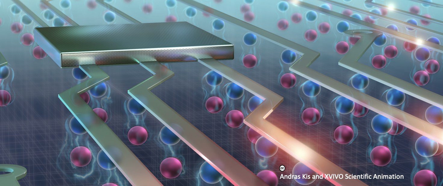
Excitonic devices based on 2D semiconductor heterostructures
2nd September 2020
Timing : 1 pm EST
For zoom link to the talks, please email mjgc@mit.edu with your institute email and mention affiliation
For a list of all talks at the NanoBio seminar Series 2020, see here
Andras Kis
Associate Professor, EPFL
Laboratory of Nanoscale Electronics and Structures
Andras Kis is an Associate Professor in Electrical Engineering at EPFL, Lausanne. He started his research group in 2008 and has made fundamental contributions to the study of the electronic properties of 2D materials and atomically thin TMDCs. His pioneering work on MoS2 transistors was the first demonstration of high-quality device on a 2D semiconductor and has been cited over 10’000 times. Andras Kis is also serving as the editor in chief of the Nature partner journal 2D materials and applications and is a highly cited researcher. Prior to joining EPFL as faculty, Kis was a postdoctoral researcher at UC Berkeley in the group of Alex Zettl. He received his Ph.D. in physics from EPFL in 2003 and received his MSc in physics from the University of Zagreb, Croatia. His major awards include the Latsis prize in 2004, ERC starting grant in 2009 and ERC consolidator grant in 2015.