|
|
|

for 6.111 Introduction to Digital Systems
6.111 home → Labkit home → Test Programs → Complete PCB Test
Complete Labkit PCB Test Procedure
by Nathan IckesIntroduction
This document describes the procedure for testing just about every function on the labkit PCB. It employs all of the main labkit test programs in a logical order, plus some additional low-level tests of the labkit's power supplies.
The major test programs have their own documentation pages, which describe the workings of the test programs in more detail, and may be helpful for debugging boards which fail one or more of these tests. These individual documentation pages also include links to the actual Verilog source code for the tests.
To help keep track of all the functions that need to be tested on each board, a test checklist is available.
Equipment Required
The following equipment is necessary in order to perform a complete checkout of the labkit PCB.
- One triple-output power supply (or equivalent individual supplies) capable of generating +5V (at 2A), +15V (at 1A), and -15V (at 1A).
- One custom power supply cable for the labkit PCB. This cable has a six-position Molex connector on one end, and four labeled banana plugs on the other.
- One digital voltmeter. (No voltages measured will be greater than 15V.)
- One Compact flash card containing the test program files.
- One PS/2 keyboard.
- Two 3.3V crystal oscillators, around 10MHz, in a full- or half-can package.
- One PC with a serial (RS-232) port and a terminal program (e.g. HyperTerm). The Xilinx iMPACT software should also be installed.
- One RS-232 null-modem cable to connect the PC's serial port to the board under test. (The board end of this cable must have a female DB9 connector.)
- One Xilinx Parallel Cable 4 JTAG programming cable.
- Two user I/O loopback test boards.
- One daughtercard loopback test board.
- Two logic analyzer loopback cables.
- One stereo audio source with line-level outputs, and RCA patch cables to connect to the board under test.
- Headphones or PC speakers with a 1/8" stereo plug.
- Cables to connect the above headphones or speakers to the labkit's RCA line-level outputs.
- One computer monitor capable of a resolution of 1024x768 at 75Hz, with a 15-pin VGA cable.
- One TV monitor, with a composite and s-video inputs, and cables to connect each input to the labkit.
- One composite video source (such as a video camera) and an RCA patch cable to connect to the board under test.
- Ons s-video source (such as a VCR), and the appropriate cable to connect it to the labkit.
Loopback fixtures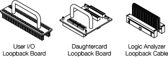
Setting Up the Compact Flash Card
The test programs will already be loaded onto the compact flash card supplied to the board assembly house. The instructions here are for the benefit of students and instructors at MIT who may want to re-run the tests in the future.
The card must be formatted with a FAT16 file system, and should contain the following directories and files
Compact flash card contents
/ (Root directory)
    xilinx.sys
    tests/
        avtest/
            avtest.ace
        cftest/
            cftest.ace
        flashtst/
            flashtest.ace
        iotest/
            iotest.ace
        memtest0/
            ram0test.ace
        memtest1/
            ram1test.ace
|
Some Notes About the Procedure Descriptions
Connectors, switches, LEDs, etc. referred to in the following procedures are referenced by their reference designators (e.g., D12 or U17). The reference designator is always silkscreened onto the PCB in small type near the respective component. Frequently, however, these components also have a more descriptive and user-friendly label that is also silkscreened on the PCB. In such cases, the more descriptive label is given in quotes after the reference designator. For example: J8 ("Mouse") and J9 ("Keyboard") are the labkit's two PS/2 connectors. Diagrams have also been provided to assist in locating some of the more esoteric components.
Each test procedure concludes with a section containing some minimal troubleshooting tips. Generally, these simply instruct the test operator to inspect the most relevant components. These are in no way exhaustive lists of the components whose malfunction could cause the tests to fail.
Testing the Onboard Power Supplies
The labkit PCB incorporates two switching power supplies that generate 1.5V and 3.3V from the incoming 5V power. This test verifies that the outputs of these supplies are within tolerance. Additionally, the power terminals for the breadboarding area are tested. These terminals supply 3.3V, 5V, 12V, and -12V. (±12V is derived from the ±15V incoming power by linear regulators.)
Equipment Required
Triple-output power supply or three individual power supplies, labkit power cable, voltmeter.
Procedure
- Set the power supplies to generate 5.0±0.1 volts, 15.0±0.5 volts and -15.0±0.5 volts.
- With the power supplies off connect the supplied power cable to the supplies and the board under test according to the diagram below.
Power supply connections
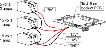
If the power supplies have an adjustable current limit, the 5 volt supply should be set to at least 2 amps, and the 15 volt and -15 volt supplies should be set to at least 1 amp.
- Turn on all three power supplies, in any order.
- On the back side of the board, measure the voltage across C420 and verify that it is between 3.0 and 3.6 volts.
Location of capacitors C420 and C423
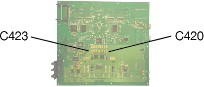
- Measure the voltage across C423 and verify that it is between 1.4 and 1.6 volts.
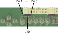
- On the front side of the board, find the five-pin connector J19. Verify the following voltage across the pins of this connector:
- Pin 1("3.3", positive lead of meter) to pin 3 ("GND", negative lead): 3.0 to 3.6 volts
- Pin 2 ("5.0", positive lead) to pin 3 ("GND", negative lead): 4.5 to 5.5 volts
- Pin 4 ("12", positive lead) to pin 3 ("GND", negative lead): 11 to 13 volts
- Pin 5 ("-12", positive lead) to pin 3 ("GND", negative lead): -11 to -13 volts
Location of J19
- Verify that all five power supply status LEDs (D14, D15, D16, D18, and D19), on the top side of the board, are on.
Troubleshooting
If the voltage across C420 is out of tolerance, inspect U26 and surrounding components. If the voltage across C423 is out of tolerance, inspect U27 and surrounding components. If any of the voltages on J19 are out of tolerance, check the continuity of fuses F1 through F4, and inspect U24, U25, and surrounding components.
Testing the FPGA and Compact Flash Interface
This tests the basic ability of the SystemACE compact flash controller chip to read a configuration file from a compact flash card and use the contents of that file to configure the FPGA.
Equipment Required
Power supply, power cable, compact flash card.
Procedure
- Connect the power supply, power cable, and PCB under test as described in the previous test.
- Set the configuration source switch S19 (near the top edge of the PCB) to "JTAG/CF".
- Turn on the 5V power supply. (The +15V and -15V supplies are not needed for this procedure.)
- Verify that D10 ("Error", a red LED near the top edge on the front side of the board) is blinking.
- Press and release S20 ("Reset"). Verify that the red FPGA status LED D20 ("In Reset") lights for about half a second after S20 is released, and that the yellow D13 below is ("Initializing") remains lit after D20 goes out.
- Set switch S18 ("Select", near the top edge of the board) to position "7", and insert the compact flash card into J16.
- Verify that the compact flash status LED D10 ("Error") goes out, and D11 ("Done", green, near D10) blinks for a second or two, and then comes on steady. Also verify that D12 ("Configured", green) comes on steady when D11 has finished blinking.
- LEDs D2 through D9, near the bottom edge of the board, should blink in a back-and-forth pattern.
Switch and LED locations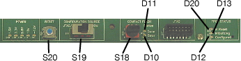
Troubleshooting
If any of the LEDs do not illuminate properly, inspect U17, U18, J16, and surrounding components.
Testing General Input and Output Ports
This is a general test of all the labkit's switches, LEDs, alphanumeric displays, logic analyzer connectors, user I/O ports, and any other non- audio and video inputs and outputs.
Equipment Required
Power supply, power cable, compact flash card, two half- or full-can crystal oscillators, two user I/O loopback boards, one daughtercard loopback board, and two logic analyzer loopback cables, PS/2 keyboard, RS-232 null-modem cable, PC with serial terminal program.
Procedure
- Connect the power supply, power cable, and PCB under test as described in the onboard power supply test.
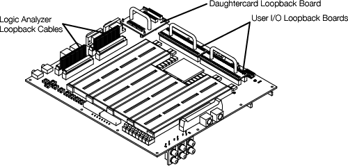
- With power to the PCB turned off, insert the two crystal oscillators in the sockets Y2 and Y3 on the front side of the PCB. The silkscreen outline illustrates the proper orientation and alignment for either full- or half-can oscillators: note the square corner.
- Install the two user I/O loopback boards: one board should bridge J10 and J11, and one board should bridge J12 and J13. With the PCB oriented breadboard side up and with the slide switches in the lower right corner, the text on the loopback boards should be right side up.
- Install the daughtercard loopback board into J14 and J15. The 22 DIP switches on the loopback board should all be set to the closed position.
- Install the logic analyzer loopback ribbon cables. One cable should connect J24 and J25, and the other cable should connect J26 and J27. The drawing below shows the labkit board with all of the loopback fixtures correctly installed.
Labkit PCB with loopback boards and cables installed
- Apply 5V power to the PCB. Set S18 ("Select") to position "0", insert the compact flash card, and wait for D11 ("Done") to finish blinking.
- Verify that the alphanumeric displays (DISP1 and DISP2) read as shown below.
Correct display contents on startup

If the last character is not "P", then the I/O loopback test of the user I/O, daughtercard, and logic analyzer connectors has failed. In such a case, the last two characters of the display will give a hexadecimal error code which can be looked up in the table in the I/O test documentation.
If the two characters after "C:" are not double-headed arrows, then one or both of the socketed oscillators are not oscillating. (The first character corresponds to the oscillator in socket Y2 and the second character to the oscillator in socket Y3.)
- Set all of the slide switches S10 through S17 ("7" through "0") to their lowest position. Verify that LEDs D2 through D9 ("7" through "0") are all off.
- One by one, flip the switches S10 through S17 up and down and verify that the corresponding LED (S10 → D2, S11 → D3,…) illuminates when each switch is high.
- With all S10-S17 low, press button S5 ("Enter") and verify that all of D2 through D9 illuminate while S5 is depressed.
- One by one press S1 through S4 ("Up", "Down", "Left", and "Right") and S6 through S9 ("3" through "0") and verify that depressing each pushbutton causes one of the LEDs D2 through D9 to blink rapidly.
- Plug the PS/2 keyboard into J9 ("Keyboard") and then press and release S5 ("Enter"). Type the letter 'a' on the keyboard and verify that the display on the PCB reads in part "K:A". (Only the keys 'a', 'b', 'c', 'd', 'e', and 'f' are recognized by the test program.)
- Unplug the keyboard and plug it into J8 ("Mouse"). Press S5 ("Enter") and then type the letter 'a' again. Verify that the display reads in part "M:A".
- Connect a null-modem serial cable from J7 ("RS-232") to the serial port. Start a serial terminal program (e.g., HyperTerm or Minicom) on the PC.
- Open a serial connection on the PC, and verify that characters typed at the console are echoed back by the labkit PCB. The TXD and RXD (and CTS and RTS) signals are simply tied together in the FPGA, so the exact communications settings used are not critical (115kbaud, 8-data bits, no-parity, for example). Hardware flow control should be turned on, to test the RTS and CTS lines.
Troubleshooting
If any of the switches or LEDs malfunctions, inspect the switch itself and resistor packs RP14 through RP16.
If either of the mouse or keyboard ports appears to be malfunctioning, try power cycling the board under test, with the keyboard plugged into the appropriate port. Sometimes the keyboard does not reset properly when hot plugged. Otherwise, inspect U12 and surrounding components.
If the I/O loopback test fails, consult the table of failure codes to identify which pin caused the failure. If failing pin is a user I/O pin, inspect the corresponding buffer IC (one of U13 through U16). If the failing pin is a part of a logic analyzer connector, inspect the associated termination resistor (R153 through R155 for the clock signals, and RP19 through RP26 for the data signals
Testing the Audio and Video Codecs
The labkit contains dedicated codecs for audio and video input and output. This test procedure verifies the ability of the labkit to generate audio and video test signals internally, and loop back test signals applied to the audio and video inputs. The loopback tests include the full decoder-FPGA-encoder datapath: the external signals are digitized, and then resynthesized.
Equipment Required
Power supply, power cable, compact flash card, headphones or amplified speakers, stereo audio source and RCA patch cables, NTSC TV monitor with composite and s-video inputs, composite video source (video camera), s-video source (VCR), VGA monitor.
Procedure
- Connect 5V power to the PCB, as described in the onboard power supply test procedure.
- Set S18 ("Select") to position "1" and insert the compact flash card. Turn on the 5V power supply if it is off, or press S20 ("Reset") if the power supply is already on. Wait for D11 ("Done") to finish blinking.
- Plug a pair of headphones or amplified speakers into J1 ("e;Headphones").
- Set slide switches S16 ("1") to the down position, and S17 ("0") to the up position. The middle portion of the alphanumeric display should read "SIL" (for "silence": no audio output).
- Press pushbutton S5 ("Enter"). A high-pitched tone should be heard in the headphones while the button is depressed. Press pushbutton S1 ("Up") a couple times to increase the output volume level, if necessary. (The first few characters of the alphanumeric display indicate the current volume level, from 0 to 15.)
- Set slide switches S16 ("1") to the up position, and S17 ("0") to the down position. The middle portion of the alphanumeric display should read "SIN", indicating that the audio codec is synthesizing a sine-wave.
- Verify that a steady, medium-pitch tone can be heard in the headphones, and that the volume of the tone can be adjusted by pressing S1 ("Up") and S2 ("Down"). The tone should be clean, with no audible hiss or static present.
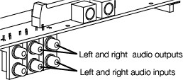
- Connect a stereo audio source to the left and right line input jacks (part of J2)
Audio input and output jacks on J2
- Set slide switches S15, S16, and S17 ("2", "1", and "0") to the down position. The middle of the alphanumeric display will read "LIN", indicating that the audio output is coming from the line-level audio input jacks.
- Verify that the audio being fed into the line input jacks can be heard in the headphones. Again, there should be no audible static or other noise present.
- Connect the headphones or speakers to the line-level output jacks (part of J2, see the above figure). Again, verify that the audio being fed into the line input jacks can be heard in the headphones.
- Connect a PC microphone to J3 ("Microphone") Set slide switch S15 ("2") to the upward position. (The middle portion of the display will read "MIC", for microphone.) Adjusting the volume as necessary with S1 and S2, verify that sounds picked up by the microphone are replayed in the headphones.
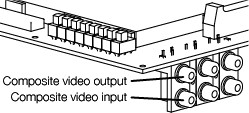
- Connect the composite input of the TV monitor to the composite video output jack (part of J2).
Composite video jacks on J2
- Set S13 (" 4") to the down position and S14 ("3") to the up position. The rightmost portion of the alphanumeric display will read "MITLOGO".
- Verify that a test pattern containing the MIT logo is displayed on the TV monitor.
TV test pattern

- Connect an s-video source to J6, the s-video video input jack.
- Set S13 and S14 ("4" and "3") to the up position. The rightmost portion of the alphanumeric display will read "S-VIDEO".
- Verify that the s-video source signal is displayed on the TV monitor.
- Connect a composite video source to the composite video input jack (part of J2, see above figure).
- Set S13 ("4") to the up position and S14 ("3") to the down position. The rightmost portion of the alphanumeric display will read "COMPOSI".
- Verify that the composite video source signal is displayed on the TV monitor.
- Disconnect the TV monitor from the PCB's composite output, and connect the monitor's s-video input to J5, the PCB's s-video input.
- Verify that the same video source signal is still displayed on the TV monitor.
- Connect a VGA-compatible monitor to J4 ("VGA").
- Verify that a test pattern containing the MIT logo is displayed on the VGA monitor.
VGA test pattern

Troubleshooting
If an audio test fails, inspect U1 and surrounding components. If a video test fails, inspect U5 and U7 and surrounding components.
Testing the SRAM
This procedure tests the synchronous SRAMs on the back side of the labkit PCB. Each of the two SRAMs is tested independently. For each SRAM, the test program begins by testing the address lines by writing 0 to the first address, 1 to the next address, and so on, up to the last addressable location. These values are then read back and verified. The data lines are then tested by a walking-one test.
Equipment Required
Power supply, power cable, compact flash card
Procedure
- Connect 5V power to the PCB, as described in the onboard power supply test procedure.
- To test memory bank 0, set S18 ("Select") to position "2" and insert the compact flash card. Turn on the 5V power supply if it is off, or press S20 ("Reset") if the power supply is already on. Wait for D11 ("Done") to finish blinking.
- Verify that LEDs D2 ("7") and D3 ("6"), near the bottom edge of the board, are illuminated.
- Set slide switch S17 ("0") to the down position. Press and release pushbutton S9 ("0") to reset the test program, and then press and release pushbutton S8 ("1") to start the test.
- Verify that the test program begins executing. The alphanumeric display will show two rapidly changing numbers. It takes approximately one minute for the test to complete.
- When the test completes, the alphanumeric display will blank and D7 ("2") will illuminate. Verify that D6 ("3") does not illuminate, which would indicate an error detected by the test.
- To test memory bank 1, change rotary switch S18 ("Select") to position "3" and press pushbutton S20 ("Reset"e;) to load the test program for the second memory bank.
- Set slide switch S17 ("0") to the down position. Press and release pushbutton S9 ("0") to reset the test program, and then press and release pushbutton S8 ("1") to start the test.
- Verify that the test program begins executing. The alphanumeric display will again show two rapidly changing numbers. It again takes approximately one minute for the test to complete.
- When the test completes, the alphanumeric display will blank and D7 ("2") will illuminate. Verify that D6 ("3") does not illuminate.
Troubleshooting
If the test of the first memory bank fails, inspect U8 and particularly resistor packs RP4 RP5, RP7, and RP8.
If the test of the second memory bank fails, inspect U9 and particularly resistor packs RP9 RP10, RP12, and RP13.
Testing the Flash Memory
This test verifies correct operation of the flash memory on the back of the labkit PCB. The test begins by erasing the entire flash chip, and then writes and reads back every location. Finally, the flash is erased again.
Equipment Required
Power supply, power cable, compact flash card
Procedure
- Connect 5V power to the PCB, as described in the onboard power supply test procedure.
- To test memory bank 0, set S18 ("Select") to position "4" and insert the compact flash card. Turn on the 5V power supply if it is off, or press S20 ("Reset") if the power supply is already on. Wait for D11 ("Done") to finish blinking.
- The test will begin automatically, as soon as the FPGA is configured. The alphanumeric display will read "ERASING" while the entire flash is erased. This takes approximately 2 minutes. The display will then read "WRITING" while every location in the flash is written to. This takes about 20 minutes. (The last address to be written is 0x7FFFFF.) The entire flash will then be read back (takes a couple seconds) and the erased again (takes another 2 minutes.
- When the test completes, the display should read "*** PASSED ***" if no errors were detected. If an error does occur, the display will read "ERR", followed by a one word description of the error. See the flash test documentation for an explanation of the possible error messages.
Troubleshooting
If the test does not succeed, inspect the flash ROM, U10.
Testing the FPGA Configuration EPROM
This tests an alternative mechanism for configuring the FPGA, using the configuration EPROM, U21. The EPROM is programmed over the JTAG bus, using the Xilinx iMPACT software, and then the PCB is tested to ensure that the FPGA successfully loads the configuration data from the EPROM.
Equipment Required
Power supply, power cable, PC with Xilinx iMPACT software installed, JTAG programming cable (Xilinx Parallel Cable 4).
Procedure
- Connect the Parallel Cable 4 JTAG cable to the parallel port and one PS/2 port of the computer. The status light on the cable should turn yellow once the power connector on the cable has been plugged into a PS/2 port.
- Connect the ribbon cable on the end of the JTAG cable to J17 on the labkit PCB.
- Apply 5V power to the PCB, as described in the onboard power supply test procedure. The status light on the JTAG cable should turn green.
- On the PC, launch the iMPACT application (On the machine supplied to the assembly house, there is a shortcut to iMPACT on the desktop. Otherwise, select iMPACT from the Start menu: Program Files→Xilinx ISE 6→Accessories→iMPACT.)
- A wizard will automatically start. In the first dialog, choose "Configure devices" (the default); in the second dialog, choose "Boundary-scan mode" (the default) and in the third dialog, choose "Automatically connect to cable and identify boundary-scan chain" (also the default).
- The software will initialize the programming cable and probe the JTAG chain, and should identify three JTAG devices. It will then prompt the user to select a programming file for each device.
- The first device (xccace) is the compact flash interface controller chip: it should be bypassed (choose "Bypass" in the file selection dialog).
- The second device (xc2v6000) is the FPGA: it too should be bypassed.
- The third device (xcf32p) is the EPROM. Assign to it the
epromtest.mcffile. (On the machine supplied to the assembly house, the file is in My Documents. It can also be downloaded here:epromtest.mcf.)
- In the graphical view of the JTAG chain, right-click on the EPROM device, choose "Program...", and click "OK" in the confirmation dialog. It takes a couple of minutes to erase and program the EPROM.
- When the programming operation has completed, turn off power to the labkit PCB. Remove any compact flash card from the labkit. Set switch S19 ("Configuration Source") to "EPROM" and turn power back on to the PCB.
- It will take approximately five seconds for the FPGA to configure itself from the data now stored in the EPROM. When configuration is complete, the green "Configured" FPGA status LED (D12) should light, and the alphanumeric display should read "MIT 6.111 LABKIT"
Troubleshooting
If the JTAG chain is not correctly identified by iMPACT, inspect U18, U21, R124 and J17. Also, be sure that U22 and R125 have not been installed.
MIT 6.111 Introduction to Digital Systems, Updated November 14, 2006