


|
<< INTRODUCTION >> << OVERVIEW >> << AUDIO >> << GAMEPLAY >> << VIDEO >> << IMPROVEMENTS >> << ZBT RAMS >> << TIPS AND TRICKS >> << NES INPUT FSM >> << TOOLS >> |
Appendix: ZBT RAMs The following table shows the control signal values needed to perform a read or a write operation on one of the ZBT SRAMs included in the kit. Note that these signals are not the signals defined on the pins of the chip but rather the interface signals defined in the labkit.v top level design file.
Because the ZBT SRAMs are pipelined, they can greatly improve access speeds over traditional SRAMs. However, this pipelining feature also makes the chips more complicated to use effectively. In general, the rule is that addresses and control signals are presented at time t and data is presented at time t + 2. In other words, a read operation will return data to the bus two clock cycles after the chip is presented with an address, and a write operation will store whatever data is on the bus two clock cycles after the write request. The figure below comes from Cypress web site, and illustrates these timing features. 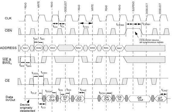
|