Post Detection Amplifier & Filter
Requirements
The TMRS-3 radiometers all have high frequency RF front ends that amplify and filter the radio-brightness signal. In order to measure the power of this signal, the output of the RF gain chain is passed through a high frequency detector diode operating as a power detector, similar to an AM radio detector. This post-detected signal contains a lot of high frequency noise and is a very low voltage. We want to use the 12-bit un-buffered analog to digital converter built into our BL1720 microcontroller, so an analog glue solution is needed.
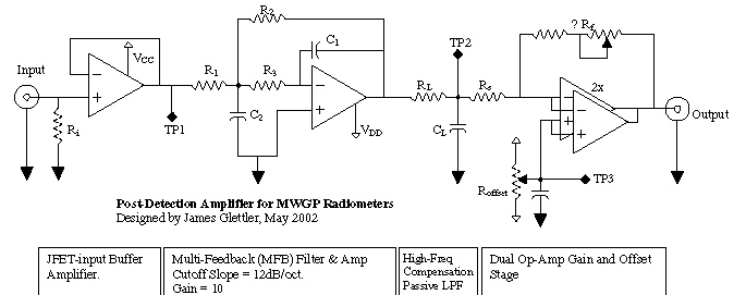
The post-detector amplifier has five purposes:
- Buffer input from detector diode
- Filter out high frequencies above Nyquist, minor integration
- Amplify signal to an acceptable range for ADC (~100X)
- Level shift signal to within ADC range
- Source enough power to drive ADC
Design
It was desirable that the post-detector amplifier be compact, easy to adjust, and very stable. To meet these conditions, and to isolate each function, a three stage, four op-amp solution was used. I chose the Texas Instruments OPA4130 quad surface mount op-amp with FET inputs. This device was selected for its stability, size, and noise. The three stages are: input buffer, low pass filter and output driver.
Click for Full Size (GIF - 18.8K)
The input buffer is a single stage voltage follower. The high input impedance of the FET op-amp doesn't load down the detector at all. One concern of course at high frequencies is proper termination of the transmission line, so a load resistor (Ri) is included if needed.
The low-pass filter block follows the buffer. This uses one op-amp in a multi-feedback (MFB) filter arrangement as described in "Active Low Pass Filter Design" from TI. It is a two pole filter with some gain that allows our output driver stage share some of the amplification requirements. A final RC low pass filter is used to remove the high frequency components that are passed through the MFB filter due to parasitic capacitance.
The driver stage takes care of the remaining necessary gain, the offset voltage, and driving the ADC. A simple variable gain inverting configuration is used, with two op-amps tied together in parallel for increased output current drive capability. The non-inverting input is connected to a variable resistor for setting the offset voltage.
Prototype
The first PDA was prototyped using dead-bug construction on an un-etched copper circuit board. The circuit was basically built upside down over the ground plane with pads made on top where needed. It was designed to have high gain and a cut off frequency of 330Hz. The prototype and frequency response are shown below.
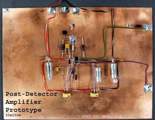
Click for Full Size (JPG - 37.7K)
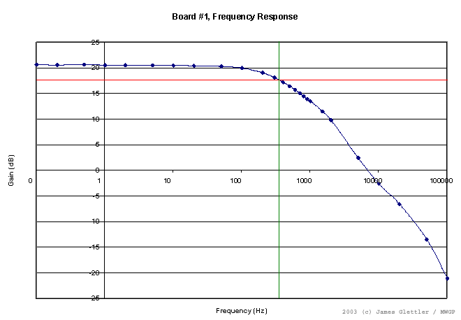
Click for Full Size (GIF - 6K)
Construction
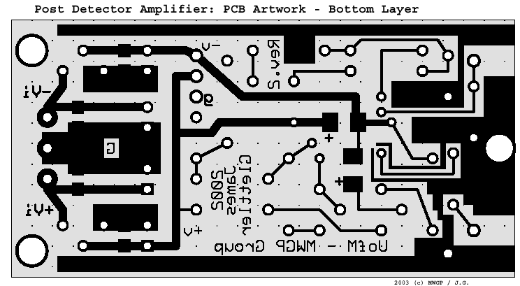
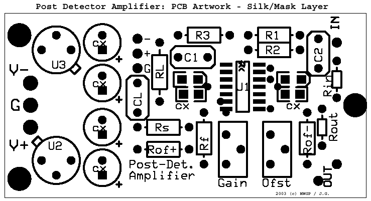
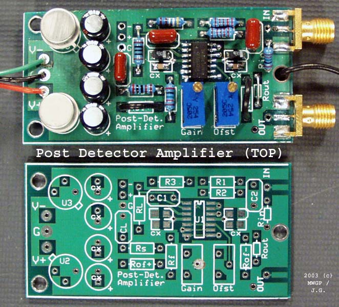
Because at least seven identical amplifiers were needed, with a number of surface mount components, it made sense to have PCBs fabricated. This was done just like the microcontroller I/O board, but with the addition of silk screen and a solder-mask. In addition to the amplifier, dual-rail regulators were added to the board to further increase noise immunity. The PCB artwork along with an empty and populated PDA board are shown below. These PCBs were laid out using ExpressPCB due to the simplicity of the design. A number of three terminal regulator (78xx/79xx) circuits were also fabricated [not shown]using extra PCB space.
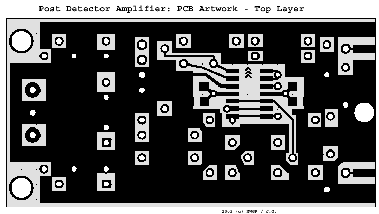 Click for Full Size (GIF - 13K) |
 Click for Full Size (GIF - 15K) |
 Click for Full Size (GIF - 15K) |
|
 Click for Full Size (JPG - 120K) |
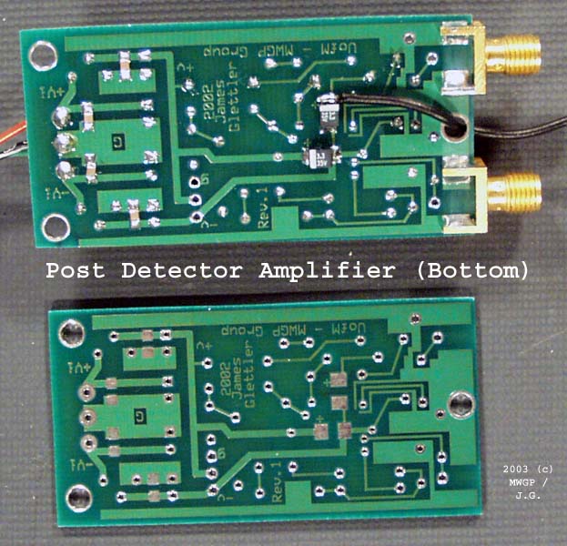 Click for Full Size (JPG - 97K) |