Interface Daughterboard
The Z-world BL1720 has a number of hardware interface features that need to be accessed easily. The I/O connections consist of four 10-pin headers and two 14-pin headers on the top of the BL1720 motherboard. In order to make use of these I/O lines, a method of easily connecting necessary electronics is needed. It must fulfil the following needs:
- Provide the bias and load voltage and resistances for the thermisters.
- Accept the data signal from the Post-RF amplifier.
- L & C band: Properly drive the DowKey RF latching switches.
- 19 & 37GHz: Translate digital output to differential TTL to drive circulators.
- Drive power relays to be connected to heaters (or fans) and provide connections for outputs.
- Provide an active-low sinking output for an external power relay.
- LED status indicators tied to digital outputs.
- Implement a 4-bit address switch to the digital inputs.
- Use a simple robust connector output to interface with radiometer electronics.
A daughterboard makes the most sense in this case. Making one board that could support multiple radiometer styles was desirable as well in order to save production costs and simplify design. The board has one D-shell connector, in this case a DB-25, for all the RF control and measurement signals. This makes wiring and maintenance easy. The power supply and power relay outputs are terminal strips. This is because these are less likely to be disconnected during maintenance and need to support higher currents.
Schematic
The following schematic implements all the features necessary for the L-band and C-band TMRS-3 radiometers. What is missing from the schematic is the logic for the differential TTL level conversion, but this is minimal.
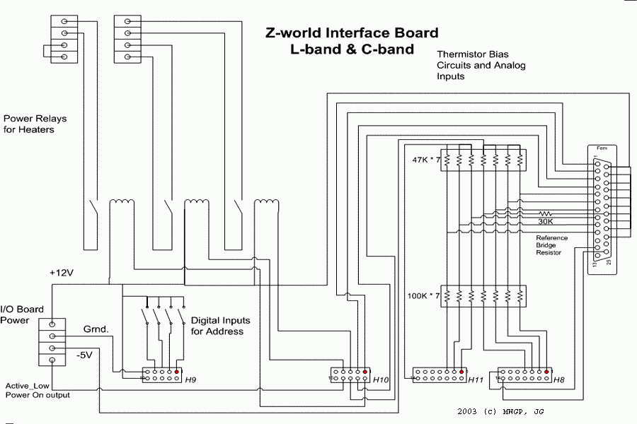
Click for Full Size (GIF - 34.5KB)
After schematic design, came board layout. The following layout is for the STAR-Light front-end based systems (L-band and C-band).
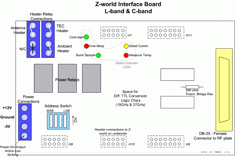
Click for Full Size (GIF - 65.7KB)
PCB Design
Because the daughterboard is relatively low speed, PCB design was simple and straightforward. Only a two layer board was used, fabricated by ExpressPCB using their software. Circuitry was included on the board to support either switches or circulators. The following graphic shows the fabrication details of each layer overlaid on each other.

Click for Full Size (GIF - 122KB)
Construction
Because the PCBs were fabricated externally, construction time was significantly reduced. There were two errors on the board that were easily correctable. The following image shows a completed daughterboard (this one for the University of Florida C-band radiometer) along with callouts to each connector.

Click for Full Size (JPG - 103KB)
The general design was prototyped prior to PCB design.
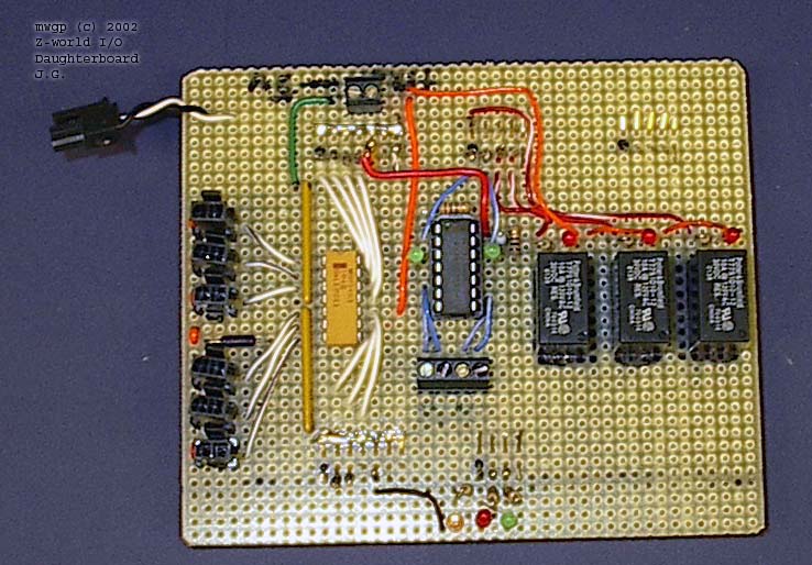
Click for Full Size (JPG - 106KB)