Power System & Regulators
The radiometer systems all require a number of DC voltages at various currents for operation. It is rather important that the power supplies are clean and low noise and are able to handle large currents where necessary. Voltages needed range include +24v, +15v, +/-12v, +6, +5.2v, +/-5v, +4.5v, 3.3v, 2.5v, 1.8v at currents in the milliamp range to the amp range. Therefore, a multi-step system was decided on.
Power enters the radiometer system's power supply box in the form of wall current from a 120V@30A AC line connected with a Marinco locking connector. This power supply box contains nine linearly regulated Acopian AC to DC supplies of various configurations providing a number of intermediate voltage levels. It also includes one 24V@50A switching power supply directly used for the thermal control systems. Fusing and cold weather heaters and the serial network distrabution is in this box as well.
A number of umbilical cables snake from the power supply box to each of the radiometer boxes. Once inside, various power supplies are fed to a number of mostly linear regulators. These regulators are almost POL (point-of-load) linear regulators to keep noise down to a minimum. All cabling is twisted pair. Care was taken to separate high noise logic supplies from low noise RF supplies all the way back to the power supply box to minimize coupling between supplies and coupling between radiometers.
POL Linear Regulators
Because some of the power supply requirements were in flux, it was difficult to determine exactly what voltages were needed where. Therefore, we decided to build a standard regulator platform that we could mount anywhere and put any standard 78xx/79xx series or equivalent regulator in. It also has reverse charge protection diodes and moderate decoupling of both the input and output. This design could be done parallel to the design and construction of more critical systems and for the most part worked well. By combining the PCB design of these mini regulator boards with the design of the Post-detector amplifier PCBs, significant costs were saved. A single POL regulator board is shown below fully populated except for the TO-220 regulator to be mounted on the right. The regulator TO-220 case could then be heatsinked to the aluminum mounting plate of any radiometer it was installed in using some Kapton (polyimide) tape for electrical isolation.
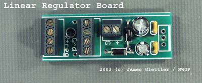
Click for Full Size (JPG - 30K)
Power System for C-band Upgrade
Originally, the C-band radiometer was scheduled to be upgraded to fully-polarimetric operation by using the entire STAR-Light backend. However, because development of that backend was temporarily suspended for various reasons, it became necessary to develop our own that would work with what we had.
Our power supply box had one 11 Amp linearly regulated 6V supply that was isolated from the rest of the radiometers to be used only for the digital correlating backend systems. From this we needed to get a good number of different voltages. The FPGA needed 5v, 3.3v, 2.5v and 1.8v of relatively stable power. The clock circuitry needed 3.3v and -5V of clean power, and each ADC needed rock steady +/-5v and 2.5v.
After some consideration, it seemed as if three different topologies could be used to meet our requirements. For output that need high power and had only minimal noise requirements, such as the FPGA, a POL integrated switching module is the easiest to implement. This is used for the 1.8V and 2.5V requirements. For outputs that have more stringent noise requirements but draw less power, a low drop out regulator can be used. Diodes are added in series with the input to reduce the power dissipation within the regulator package. Finally, for negative voltages where noise is very important (specifically the -5V), a switching module is used to generate a negative voltage that is then linearly regulated to -5V.
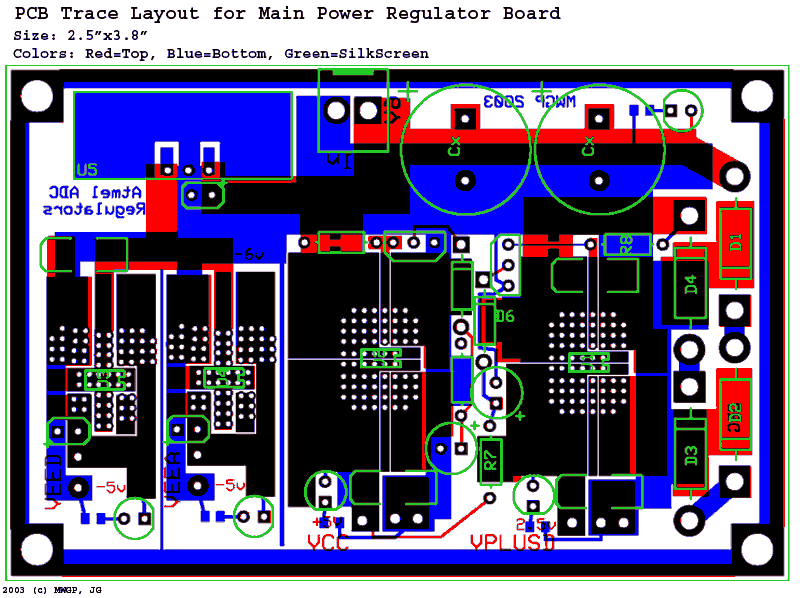
It made sense to put the regulators as close the loads as possible but on separate boards for noise and construction reasons. Therefore three boards will be used in the end, one correlator power board for the FPGA and clock, and two ADC power supply boards. Below are the schematics and PCB layouts for each. Notice in the PCB layout that the surface mount regulators are given a large amount of copper surface area and vias for power dissipation.
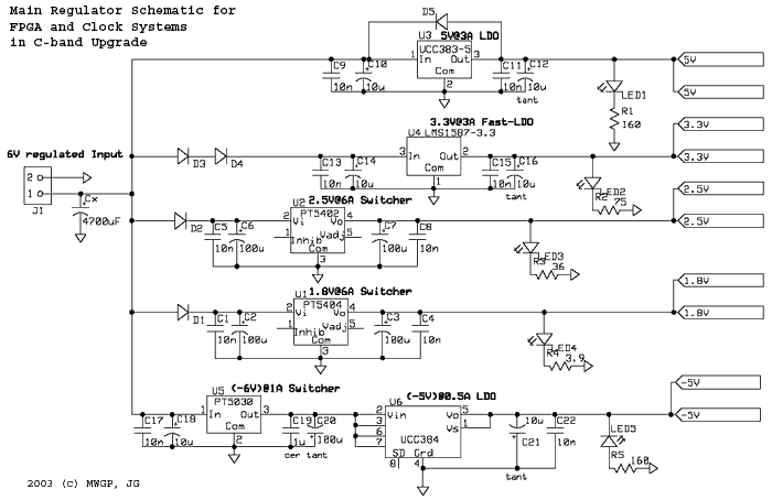 Main Power Regulators Schematic (GIF - 17.4K) |
 ADC Power Regulators Schematic (GIF - 18K) |
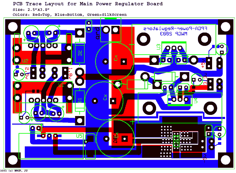 Main Power Regulators PCB (GIF - 38K) |
 ADC Power Regulators PCB (GIF - 42K) |