
A first-ever complete map for elastic strain engineering
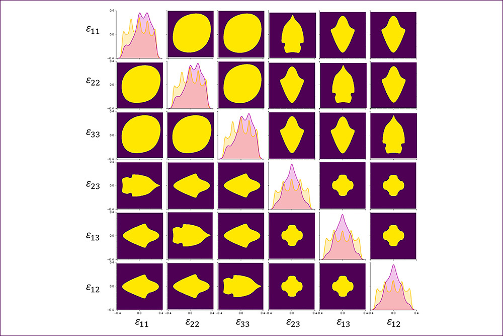
The “map”, or the phonon stability boundary, a graphical representation that plots the stability regions of a crystal as a function of strain. This map helps scientists and engineers determine the conditions under which a material can exist in a particular phase and when it might fail or transition to another phase. By analyzing the phonon stability boundary, researchers can understand material properties at extreme conditions and design new materials with desired characteristics. Graphic courtesy of the researchers
Without a map, it can be just about impossible to know not just where you are, but where you’re going, and that’s especially true when it comes to materials properties.
For decades, scientists have understood that, while bulk materials behave in certain ways, those rules can break down for materials at the micro- and nano-scales, and often in surprising ways. One of those surprises was the finding that, for some materials, applying even modest strains — a concept known as elastic strain engineering — on materials can dramatically improve certain properties, provided those strains stay elastic and do not relax away by plasticity, fracture, or phase transformations. Micro- and nano-scale materials are especially good at holding applied strains in the elastic form.
Precisely how to apply those elastic strains (or equivalently, residual stress) to achieve certain material properties, however, had been less clear — until recently.
Using a combination of first principles calculations and machine learning, a team of MIT researchers has developed the first-ever map of how to tune crystalline materials to produce specific thermal and electronic properties.
Led by Ju Li, the Battelle Energy Alliance Professor in Nuclear Engineering and Professor of Materials Science and Engineering, the team described a framework for understanding precisely how changing the elastic strains on a material can fine-tune properties like thermal and electrical conductivity. The work is described in a paper published in PNAS.
“For the first time, by using machine learning, we’ve been able to delineate the complete 6-dimensional boundary of ideal strength, which is the upper limit to elastic strain engineering, and create a map for these electronic and phononic properties,” Li said. “We can now use this approach to explore many other materials. Traditionally, people create new materials by changing the chemistry.”
“For example, with a ternary alloy, you can change the percentage of two elements, so you have two degrees of freedom,” he continued. “What we’ve shown is that diamond, with just one element, is equivalent to a six-component alloy, because you have six degrees of elastic strain freedom you can tune independently.”
Small strains, big material benefits
The paper builds on a foundation first laid as far back as the 1980s, when researchers first discovered that the performance of semiconductor materials doubled when a small — just one percent — elastic strain was applied to the material.
While that discovery was quickly commercialized by the semiconductor industry and today is used to increase the performance of microchips in everything from laptops to cell phones, that level of strain is very small compared to what we can achieve now, said Subra Suresh, the Vannavar Bush Professor of Engineering Emeritus.
In a 2018 Science paper, Suresh, Dao and colleagues demonstrated that one percent strain was just the tip of the iceberg.
As part of a 2018 study, Suresh and colleagues demonstrated for the first time that diamond nano-needles could withstand elastic strains of as much as 9 percent and still return to their original state. Later on, several groups independently confirmed that microscale diamond can indeed elastically deform by approximately 7 percent in tension reversibly.
“Once we showed we could bend nano-scale diamonds and create strains on the order of nine or 10 percent, the question was what do you do with it,” Suresh said. “It turns out diamond is a very good semiconductor material…and one of our questions was if we can mechanically strain diamond, can we reduce the band gap from 5.6 electron-volts to two or three? Or can we get it all the way down to zero, where it begins to conduct like a metal?”.
To answer those questions, the team first turned to machine learning in an effort to get a more precise picture of exactly how strain altered material properties.
“Strain is a big space,” Li explained. “You can have tensile strain, you can have shear strain in multiple directions, so it’s a six-dimensional space, and the phonon band is three dimensional, so in total there are nine tunable parameters. So, we’re using machine learning, for the first time, to create a complete map for navigating the electronic and phononic properties and identify the boundaries.”
Armed with that map, the team subsequently demonstrated how strain could be used to dramatically alter diamond’s semiconductor properties.
“Diamond is like the Mt. Everest of electronic materials,” Li said. “Because it has very high thermal conductivity, very high dielectric breakdown strengths, a very big carrier mobility. What we have shown is we can controllably squish Mt. Everest down…so we show that by strain engineering you can either improve diamond’s thermal conductivity by a factor of two, or make it much worse, by a factor of 20.”
New map, new applications
Going forward, the findings could be used to explore a host of exotic material properties, Li said, from dramatically reduced thermal conductivity to superconductivity.
“Experimentally, these properties are already accessible with nano-needles and even micro-bridges,” he said. “And we have seen exotic properties, like reducing diamond’s (thermal conductivity) to only a few hundred Watts per meter-Kelvin. Recently, people have shown that you can produce room temperature superconductors with hydrides if you squeeze them to a few hundred gigapascals, so we have found all kinds of exotic behavior once we have the map.”
The results could also influence the design of next-generation computer chips capable of running much faster and cooler than today’s processors, as well as quantum sensors and communication devices. As the semiconductor manufacturing industry moves to denser and denser architectures, Suresh said the ability to tune a material’s thermal conductivity will be particularly important for heat dissipation.
While the paper could inform the design of future generations of microchips, Zhe Shi, a postdoc in Li’s lab and first author of the paper said more work will be needed before those chips find their way into the average laptop or cell phone.
“We know that one percent strain can give you an order of magnitude increase in the clock speed of your CPU,” Shi said. “There are a lot of manufacturing and device problems that need to be solved in order for this to become realistic, but I think it’s definitely a great start. It’s an exciting beginning to what could lead to significant strides in technology.”
This work was supported with funding from the Defense Threat Reduction Agency, an NSF Graduate Research Fellowship, the Nanyang Technological University School of Biological Sciences, the National Science Foundation, the MIT Vannevar Bush Professorship and a Nanyang Technological University Distinguished University Professorship.
Written by Peter Reuell. March 2024
Department of Nuclear Science & Engineering
Massachusetts Institute of Technology
77 Massachusetts Avenue, 24-107 (map)
Cambridge, MA 02139
nse-info@mit.edu