Integrated Optical Logic
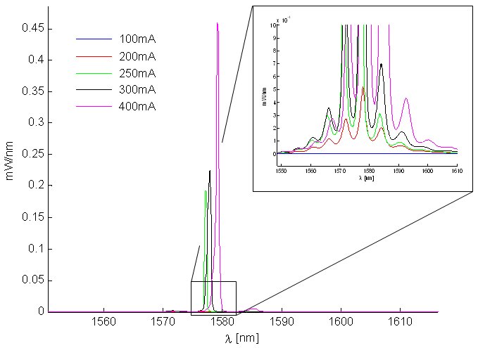
Figure 1) The lasing spectrum of a non-AR-coated 850 micron x 4 micron SOA biased at different currents.
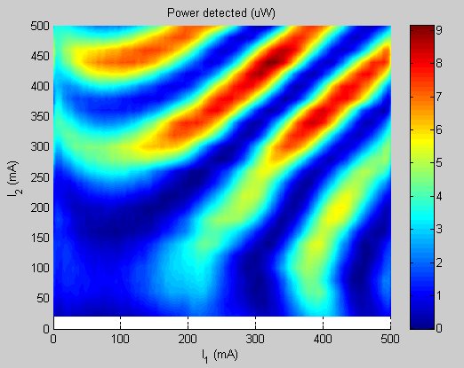
Figure 2) The static bias scan shows the interference between the two MZI arms. The x and y axes are the current that is injected into the SOA in each arm of the MZI, with the color axis being the detected output power in microwatts.
Two generations of integrated all-optical logic chips, that operate at the telecommunications wavelength of 1550 nm, have been modeled, designed, fabricated, and are being tested. The SOAs are vertically integrated with the passive waveguides using the asymmetric twin waveguide technique. The total fabrication process consists of three contact photolithography steps and associated etch and deposition steps. Semiconductor etching is performed with an inductively-coupled plasma reactive ion etcher. The metal contacts are deposited using gold plating, after which the samples are thinned and cleaved into 2 mm by 3 mm chips. The passive waveguide losses were measured to be 0.9 cm-1. Coupling losses are estimated to be approximately 7 dB per facet, due to the asymmetric shape of the waveguide mode. Lasing has been observed for non-antireflective-coated SOAs that are coupled to the passive waveguides, with the lasing threshold close to 200 mA as shown in Figure 1. Antireflective coatings were deposited onto the facets to allow for single-pass functionality measurements of the logic gates. Currently, the switching behavior is being measured. Figure 2 shows a static bias scan that is performed by measuring the transmitted power of the 1550nm light after it travels through the MZI for different combinations of SOA bias currents. The static bias scan is used to determine the bias point of the all-optical logic gate. For example, if destructive interference is desired during the "off" state of the MZI, an operating point with strong destructive interference (blue) can be chosen. If constructive interference is desired during the "off" state of the MZI, a bias point of strong constructive interference (red) can be used. Future work will include the implementation of quantum dots within the active regions of the SOAs to further increase the optical data bit rates.
