Long Wavelength Antimony-Based Devices
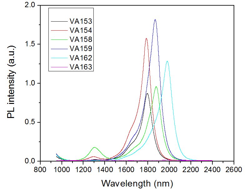
Figure 1) Compilation of PL spectra from numerous laser structures.
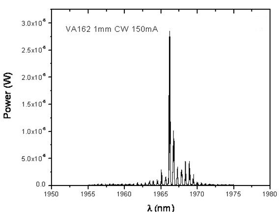
Figure 2) Optical power spectrum of a laser with two strained InGaAs quantum wells.
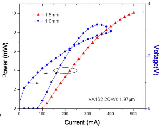
Figure 3) Continuous wave L-I-V curve at room temperature for the laser with two strained InGaAs quantum wells.
The laser structures were composed of strained InGaAs QWs with barriers of In0.48Ga0.42Al0.1As and that are sandwiched between In0.48Ga0.42Al0.1As waveguide layers. InP acts as the cladding layers in these separate confinement heterostructures. Figure 1 shows that the PL emission wavelength increases from 1790 nm to 1970 nm with increasing indium, or equivalently strain, in the QWs.
For the laser that emitted at 1966nm, Figure 2 shows the continuous-wave room temperature optical spectrum while Figure 3 shows the L-I-V curve. The maximum output power of this laser was 10 mW. The internal loss and current injection efficiency were calculated to be 44.3 cm-1 and 67.4%, respectively from 1.0mm and 1.5mm long devices. The laser was driven by a continuous current source and was mounted epi-side down to minimize heating effects. This 1.97 micron emitting laser is being mounted in a butterfly package with a fiber pig-tail, to allow the laser to be used in a photo-acoustic spectroscopy cell for petrochemical trace gas sensing.
