Equipment
| Lab and Coral Name | ICL / P10 |
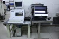
| Model | Tencor/Prometrix P-10 |
| Specialist | Bernard Alamariu (Eric Lim) |
| Physical Location | 2F 1-South Metrology |
Classification
| Process Category | Metrology |
| Subcategory | Profile |
| Material Keywords | None |
| Sample Size | 6" Wafers |
| Alternative | dektak, AFM |
| Keywords | single wafer, manual load, top side of sample, manual operation, alignment |
Description
The P10 is a stylus (contact) profilometer that is used to measure the surfacce height differences (steps) on samples. This system operates by the stylus physically making contact with the sample surface to measure changes in surface height. This tool is only allowed for Au free samples. In, GaN, or other related materials are not allowed.
| Best for | CMOS compatible patterns (PR, dielectrics or CMOS metals) |
| Limitations | Can not measure very small setps on the surface (< 50 nm). For such purposes use AFM. |
| Characteristics/FOM | Stylus tip moves over the surface to map the surface topography |
| Caution with | Sample surface should be hard enough to avoid any deposits over the tip (e.g if PR is not sufficiently bakes). If not properly handled, the tip may break. |
| Machine Charges | 5/hour |
Documents
Process Matrix Details
Permitted
Not Allowed
Ever been in EMLSamples from EML are never permitted to return to ICL or TRL
For more details or help, please consult PTC matrix, email ptc@mtl.mit.edu, or ask the research specialist (Bernard Alamariu)