Equipment
| Lab and Coral Name | ICL / endura |
| Model | AMAT Endura |
| Specialist | Paudely Zamora (Eric Lim) |
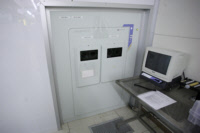
| Physical Location | 2F 1-North Deposition |
Classification
| Process Category | Deposition |
| Subcategory | Sputter |
| Material Keywords | CMOS Metals |
| Sample Size | 6" Wafers, Pieces Require Puck |
| Alternative | ICL / eBeam-EVO |
| Keywords | multi wafer, load lock, top side of sample, conformal dep, vacuum, plasma, requires flat |
Description
The endura is a GREEN metal sputtering system that sputters Ti, TiN, Al, and Al/Si. The tool is fully automatic and takes pieces (on a puck) and 6" wafers. The tool has the ability to quickly deposit thick amounts of metals and can to a certain extent deposit small thicknesses, although the accuracy may not be as good. The thicknesses in the tool are preset and therefore different thicknesses need to be coordinated with the staff. The system also contains a sputter-clean chamber, which can help to clean the surface and remove passivation layers when depositing metal onto metal. The tool runs a sequencer and is able to deposit metal film stacks. Typical throughput is 15-25 wafers per hour, but obviously depending on the metal and thickness required.
| Best for | CMOS compatible metal deposition, high throughput and very fast deposition |
| Limitations | Metal choices and recipe flexibility are limited |
| Characteristics/FOM | |
| Caution with | Pneumatic load lock |
| Machine Charges | 10/wafer + 80/um** |
Documents
SOP
| Endura | SOP for the Endura sputterer |
| Hockey Pucks | How to make hockey pucks for the Endura |
Process Matrix Details
Permitted
Been in the ALDSamples that have been in any of the ALD systems
, Germanium on surfaceSamples with germanium on the surface (typically grown films)
, Germanium buriedSamples with germanium buried below a different film
, PiecesWafer pieces may not be handled by the equipment, and are harder to thoroughly clean - preventing them from running in certain tools.
, Any exposure to CMOS metalIf the sample had ever seen a CMOS metal (or a tool that accepts CMOS metal), then some frontend tools could be contaminated by this.
(Adds), CMOS metal on surfaceCMOS compatible metals exposed on the surface. These are Al,Ni,Pt,Ti,TiN. Other metals such as Au are *NOT* part of this.
(Adds), CMOS metal buriedCMOS compatible metals covered entirely by a different material. These are Al,Ni,Pt,Ti,TiN. Other metals such as Au are *NOT* part of this.
, Been in the STS DRIEThe DRIE etch leaves behind polymer residues on the sidewall ripples, which can be a contamination concern for some tools.
, Been in the SEMA sample viewed in the SEM must have used the appropriate chuck to avoid cross-contamination
(With Appropriate Chuck), Been in the Concept1The Concep1 deposits dielectrics on GREEN wafers, however it also accepts metal and there can be cross-contamination for diffusion area
, Coming from KOHAfter a KOH etch, the samples must receive a special clean because the K ions are highly contaminating to CMOS frontend tools
, Coming from CMPAfter a CMP, the samples must receive a special clean, because the slurry residues otherwise introduce contamination and particles.
Not Allowed
Ever been in EMLSamples from EML are never permitted to return to ICL or TRL
, Pyrex SubstratesPyrex substrates can be a concern due to high sodium content, which contaminates CMOS frontend tools
, III-V SubstratesAny III-V substrates, e.g. GaAs, GaN, InP, and so on. Note though that many common III-V substrates will also carry the Au flag, but there are some GREEN III-V substrates.
, Gold or RED color codeRED color code substrates. These are gold-contaminated or have been processed in gold contaminated tools. Gold and other metals can contaminate silicon devices (GREEN color code) and have to be separated.
, Has PhotoresistSamples with photoresist cannot be exposed to high temperatures, which is typical in deposition tools. Outgassing can be a concern.
, Has PolyimidePolyimide is a very chemically resistant polymer, and can tolerate higher temperatures but cannot be exposed to typical PECVD deposition temperatures or diffusion furnaces. Outgassing can be a concern.
, Has Cured SU8Not fully cured SU8 residues can heavily contaminated plasma chambers or destroy other user's samples, but fully cured SU8 is permitted in certain tools.
For more details or help, please consult PTC matrix, email ptc@mtl.mit.edu, or ask the research specialist (Paudely Zamora)