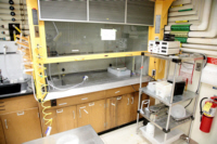
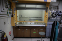
Equipment
| Lab and Coral Name | TRL / 2Dtransfer-platingHood |
| Model | Semifab WPS-400 |
| Specialist | Scott Poesse (Timothy Turner) |
| Physical Location | 5F 3-South Packaging |
Classification
| Process Category | Wet |
| Subcategory | Acids |
| Material Keywords | CMOS Metals, Non-CMOS Metals, Acids |
| Sample Size | 6" Wafers, 4" Wafers, Pieces |
| Alternative | None |
| Keywords | single wafer, both sides of sample, conformal dep, temperature, manual operation |
Description
The 2Dtransfer-platingHood is a wet station that allows for Au, Ni & Cu plating. Wafers are submerged into the plating bath, with the cathode connection clipped to the wafer, and a metal anode in the bath. Applying a voltage between anode and cathode results in electrodeposition of the metal on the wafer. Typically, a thin metal seed layer is required on the wafer, to allow conduction from the clip to the actual plating sites. Photoresist is a convenient way to mask the seed, in order to selectively plate on only parts of the wafer. The mask and seed are then removed after deposition is completed. Surface cleanliness and proper selection of seed layer is important. Usually the thin seed layer is identical to the metal being plated. If a different metal is used, make sure that it can act as a seed. A pulsed power supply can allow different plating conditions by alternating plating and un-plating cycles.
| Best for | Electrolytic plating of gold, nickel or copper. Ideal for uniform coating of surfaces, thick metal film depositions, possibly using wafers with photo resist masks |
| Limitations | Electrolytic plating requires a seed metal layer, and if patterned it needs a subsequent seed removal (typically a wet etch) |
| Characteristics/FOM | |
| Caution with | Plating baths are corrosive and toxic, proper hazardous waste disposal must be followed (never pour into sink!). Gold plating bath is cyanide based. IMPORTANT: if any acids come into contact with gold cyanide baths, deadly cyanide gas is released. It is absolutely critical not to use any acids near gold plating. Nickel and copper plating baths are acidic. So don't plate gold while plating Ni or Cu. EVER! |
| Machine Charges | 25/run |
Documents
SOP
| Wet Processing | Rules and guidelines for wet processing |
Documents
| Etch rates part 2 | Berkeley etch rate paper |
Process Matrix Details
Permitted
Been in the ALDSamples that have been in any of the ALD systems
, III-V SubstratesAny III-V substrates, e.g. GaAs, GaN, InP, and so on. Note though that many common III-V substrates will also carry the Au flag, but there are some GREEN III-V substrates.
, Germanium on surfaceSamples with germanium on the surface (typically grown films)
, Germanium buriedSamples with germanium buried below a different film
, PiecesWafer pieces may not be handled by the equipment, and are harder to thoroughly clean - preventing them from running in certain tools.
, Gold or RED color codeRED color code substrates. These are gold-contaminated or have been processed in gold contaminated tools. Gold and other metals can contaminate silicon devices (GREEN color code) and have to be separated.
(Adds), Any exposure to CMOS metalIf the sample had ever seen a CMOS metal (or a tool that accepts CMOS metal), then some frontend tools could be contaminated by this.
, CMOS metal on surfaceCMOS compatible metals exposed on the surface. These are Al,Ni,Pt,Ti,TiN. Other metals such as Au are *NOT* part of this.
, CMOS metal buriedCMOS compatible metals covered entirely by a different material. These are Al,Ni,Pt,Ti,TiN. Other metals such as Au are *NOT* part of this.
, Been in the STS DRIEThe DRIE etch leaves behind polymer residues on the sidewall ripples, which can be a contamination concern for some tools.
, Been in the SEMA sample viewed in the SEM must have used the appropriate chuck to avoid cross-contamination
, Been in the Concept1The Concep1 deposits dielectrics on GREEN wafers, however it also accepts metal and there can be cross-contamination for diffusion area
, Has PhotoresistSamples with photoresist cannot be exposed to high temperatures, which is typical in deposition tools. Outgassing can be a concern.
, Has PolyimidePolyimide is a very chemically resistant polymer, and can tolerate higher temperatures but cannot be exposed to typical PECVD deposition temperatures or diffusion furnaces. Outgassing can be a concern.
, Coming from KOHAfter a KOH etch, the samples must receive a special clean because the K ions are highly contaminating to CMOS frontend tools
(Adds), Coming from CMPAfter a CMP, the samples must receive a special clean, because the slurry residues otherwise introduce contamination and particles.
Not Allowed
Ever been in EMLSamples from EML are never permitted to return to ICL or TRL
, Pyrex SubstratesPyrex substrates can be a concern due to high sodium content, which contaminates CMOS frontend tools
, Has Cured SU8Not fully cured SU8 residues can heavily contaminated plasma chambers or destroy other user's samples, but fully cured SU8 is permitted in certain tools.
For more details or help, please consult PTC matrix, email ptc@mtl.mit.edu, or ask the research specialist (Scott Poesse)