Equipment
| Lab and Coral Name | ICL / VTR |
| Model | SVG/Thermco 7000 |
| Specialist | Robert Bicchieri (Kristofor Payer) |
| Physical Location | 2F 4-North Diffusion |
Classification
| Process Category | Diffusion |
| Subcategory | CVD |
| Material Keywords | SiNx |
| Sample Size | 6" Wafers, 4" Wafers, Pieces Require Puck |
| Alternative | none |
| Keywords | multi wafer, manual load, both sides of sample, conformal dep, vacuum, plasma, temperature |
Description
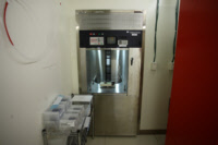
The VTR is a vertical-loading, low-pressure CVD reactor that deposits low-stress silicon nitride. The reactor flows dichlorosilane and ammonia gases at a 10:1 ratio at high temperature and low pressure which deposits a silicon-rich nitride film that has low (tensile) stress. VTR nitride is commonly used as a KOH etch mask and the deposited film is extremely conformal to topographic features on the wafer. The nitride film has a lower etch rate in HF than stoichiometric nitride (6D-Nitride) or PECVD nitride (DCVD or concept1), however it will still etch appreciably in concentrated HF. The film can also be stripped with Hot Phosphoric Acid (nitrEtch-HotPhos). The VTR is only staff-run, and an appointment needs to be made in advance with Bob Bicchieri and Kris Payer.
| Best for | Deposition of low-stess, silicon rich nitride films. Used e.g. as KOH hard mask. |
| Limitations | Staff-run tool, appointments must be scheduled ahead of time. Maximum thickness 2um. Films thicker than 1um can only be deposited on certain days. |
| Characteristics/FOM | Gases: DCS, NH3, N2. Deposition rate approximately 35 A/min. Refractive Index ~2.3. Tensile stress ~300 MPa |
| Caution with | Appointments should be coordinated with BOTH Bob Bicchieri and Kris Payer |
| Machine Charges | 65/run + 70/um |
Documents
Process Matrix Details
Permitted
Germanium buriedSamples with germanium buried below a different film
, Been in the STS DRIEThe DRIE etch leaves behind polymer residues on the sidewall ripples, which can be a contamination concern for some tools.
(With Appropriate Chuck), Been in the SEMA sample viewed in the SEM must have used the appropriate chuck to avoid cross-contamination
(With Appropriate Chuck), Coming from KOHAfter a KOH etch, the samples must receive a special clean because the K ions are highly contaminating to CMOS frontend tools
, Coming from CMPAfter a CMP, the samples must receive a special clean, because the slurry residues otherwise introduce contamination and particles.
Not Allowed
Ever been in EMLSamples from EML are never permitted to return to ICL or TRL
, Been in the ALDSamples that have been in any of the ALD systems
, Pyrex SubstratesPyrex substrates can be a concern due to high sodium content, which contaminates CMOS frontend tools
, III-V SubstratesAny III-V substrates, e.g. GaAs, GaN, InP, and so on. Note though that many common III-V substrates will also carry the Au flag, but there are some GREEN III-V substrates.
, Germanium on surfaceSamples with germanium on the surface (typically grown films)
, PiecesWafer pieces may not be handled by the equipment, and are harder to thoroughly clean - preventing them from running in certain tools.
, Gold or RED color codeRED color code substrates. These are gold-contaminated or have been processed in gold contaminated tools. Gold and other metals can contaminate silicon devices (GREEN color code) and have to be separated.
, Any exposure to CMOS metalIf the sample had ever seen a CMOS metal (or a tool that accepts CMOS metal), then some frontend tools could be contaminated by this.
, CMOS metal on surfaceCMOS compatible metals exposed on the surface. These are Al,Ni,Pt,Ti,TiN. Other metals such as Au are *NOT* part of this.
, CMOS metal buriedCMOS compatible metals covered entirely by a different material. These are Al,Ni,Pt,Ti,TiN. Other metals such as Au are *NOT* part of this.
, Been in the Concept1The Concep1 deposits dielectrics on GREEN wafers, however it also accepts metal and there can be cross-contamination for diffusion area
, Has PhotoresistSamples with photoresist cannot be exposed to high temperatures, which is typical in deposition tools. Outgassing can be a concern.
, Has PolyimidePolyimide is a very chemically resistant polymer, and can tolerate higher temperatures but cannot be exposed to typical PECVD deposition temperatures or diffusion furnaces. Outgassing can be a concern.
, Has Cured SU8Not fully cured SU8 residues can heavily contaminated plasma chambers or destroy other user's samples, but fully cured SU8 is permitted in certain tools.
For more details or help, please consult PTC matrix, email ptc@mtl.mit.edu, or ask the research specialist (Robert Bicchieri)