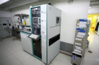
Equipment
| Lab and Coral Name | ICL / concept1 |
| Model | Novellus Concept 1 |
| Specialist | Paudely Zamora (Eric Lim) |
| Physical Location | 2F 1-North Deposition |
Classification
| Process Category | Deposition |
| Subcategory | PECVD |
| Material Keywords | SiO2, SiNx, Dielectrics |
| Sample Size | 6" Wafers, Pieces Require Puck |
| Alternative | ICL / DCVD |
| Keywords | multi wafer, load lock, top side of sample, conformal dep, vacuum, plasma, temperature |
Description
The Concept1 is a PECVD tool for depositing dielectric films on 6" wafers. It allows CMOS compatible metals, making it suitable for backend processes. It is capable of thick films in excess of 1 um, and the system deposits on multiple wafers in parallel in a batch-type reactor. A surface clean of samples or a densification anneal are not required, but can help improve adhesion and film quality for some applications. Mixed RF frequencies allow stress-balanced nitride and TEOS films. TEOS runs at 350C, and temperature adjustments will require additional time before and after the run.
| Best for | Dielectric deposition, thick films, depsoiting over CMOS metal, zero-stress nitride and TEOS films |
| Limitations | Processing of 4" wafers or pieces is possible but requires staff assistence and tool modification, and using alternative tools is recommended for those sample sizes. Recipes can only be edited by staff. Double sided polished wafers (especially with dielectric films on backside) can fall off the robot arm at unload. While regular thickness wafers often survive this drop, thinner wafers will break. For such DSP wafers, other PECVD tools such as the DCVD may be a better choice. |
| Characteristics/FOM | Chamber processes 6 wafers in parallel, typical temperature 400C. SiO2, SiN, SiOxNy, TEOS (at 350C), PSG |
| Caution with | Stand back from pneumatic loadlock during loading and unloading to avoid injury: Do not take cassette in and out while loadlock door is closing. |
| Machine Charges | 7/wafer + 1/um |
Documents
SOP
| Concept1 | SOP for the concept1 CVD |
Process Matrix Details
Permitted
Been in the ALDSamples that have been in any of the ALD systems
, Germanium on surfaceSamples with germanium on the surface (typically grown films)
, Germanium buriedSamples with germanium buried below a different film
, PiecesWafer pieces may not be handled by the equipment, and are harder to thoroughly clean - preventing them from running in certain tools.
(A), Any exposure to CMOS metalIf the sample had ever seen a CMOS metal (or a tool that accepts CMOS metal), then some frontend tools could be contaminated by this.
, CMOS metal on surfaceCMOS compatible metals exposed on the surface. These are Al,Ni,Pt,Ti,TiN. Other metals such as Au are *NOT* part of this.
, CMOS metal buriedCMOS compatible metals covered entirely by a different material. These are Al,Ni,Pt,Ti,TiN. Other metals such as Au are *NOT* part of this.
, Been in the STS DRIEThe DRIE etch leaves behind polymer residues on the sidewall ripples, which can be a contamination concern for some tools.
, Been in the SEMA sample viewed in the SEM must have used the appropriate chuck to avoid cross-contamination
(With Appropriate Chuck), Been in the Concept1The Concep1 deposits dielectrics on GREEN wafers, however it also accepts metal and there can be cross-contamination for diffusion area
(Adds), Coming from KOHAfter a KOH etch, the samples must receive a special clean because the K ions are highly contaminating to CMOS frontend tools
, Coming from CMPAfter a CMP, the samples must receive a special clean, because the slurry residues otherwise introduce contamination and particles.
Not Allowed
Ever been in EMLSamples from EML are never permitted to return to ICL or TRL
, Pyrex SubstratesPyrex substrates can be a concern due to high sodium content, which contaminates CMOS frontend tools
, III-V SubstratesAny III-V substrates, e.g. GaAs, GaN, InP, and so on. Note though that many common III-V substrates will also carry the Au flag, but there are some GREEN III-V substrates.
, Gold or RED color codeRED color code substrates. These are gold-contaminated or have been processed in gold contaminated tools. Gold and other metals can contaminate silicon devices (GREEN color code) and have to be separated.
, Has PhotoresistSamples with photoresist cannot be exposed to high temperatures, which is typical in deposition tools. Outgassing can be a concern.
, Has PolyimidePolyimide is a very chemically resistant polymer, and can tolerate higher temperatures but cannot be exposed to typical PECVD deposition temperatures or diffusion furnaces. Outgassing can be a concern.
, Has Cured SU8Not fully cured SU8 residues can heavily contaminated plasma chambers or destroy other user's samples, but fully cured SU8 is permitted in certain tools.
For more details or help, please consult PTC matrix, email ptc@mtl.mit.edu, or ask the research specialist (Paudely Zamora)