Equipment
| Lab and Coral Name | ICL / asher-ICL |
| Model | Matrix 106 |
| Specialist | Paul Tierney (Robert Bicchieri) |
| Physical Location | 2F 3-South Photo |
Classification
| Process Category | Photo |
| Subcategory | Clean |
| Material Keywords | Photoresist, EBL Resist |
| Sample Size | 6" Wafers, 4" Wafers |
| Alternative | TRL / asher-TRL |
| Keywords | multi wafer, top side of sample, isotropic etch, vacuum, plasma, temperature |
Description
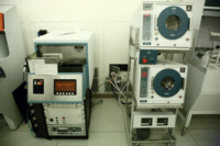
The asher-ICL is an oxygen plasma photoresist stripper that processes wafers from a casette, either individually or sequentially in automatic mode. It is similar to the asherMatrix-TRL but for GREEN processes only. However, this version has a heated chuck. Depending on the resist, typical ash times range from 2-6 minutes per wafer. Very short ashes (e.g. 10 seconds) can be used as de-scum clean procedures, although for those situations the asher-TRL is more commonly used as it is less powerful. Ashing thick resist can take longer particularly around the edges (either due to weaker plasma and/or edge beads in the resist). If surface cleanliness is critical, ashing can be followed by a piranha clean to remove trace metallic contaminants that remain on the wafer surface after ashing. Raised pins can allow some plasma access to the backside, and reduce the etch rate (as the wafer is not in contact with the heated chuck).
| Best for | Removing resist from wafers |
| Limitations | Does not remove resist from wafer backside (use asher-TRL in those situations) |
| Characteristics/FOM | O2, 400W power, 220C heated chuck. |
| Caution with | Please put system into standby after use, in order to close chamber door. |
| Machine Charges | 2/run |
Documents
Process Matrix Details
Permitted
Been in the ALDSamples that have been in any of the ALD systems
, Germanium on surfaceSamples with germanium on the surface (typically grown films)
, Germanium buriedSamples with germanium buried below a different film
, Any exposure to CMOS metalIf the sample had ever seen a CMOS metal (or a tool that accepts CMOS metal), then some frontend tools could be contaminated by this.
, CMOS metal on surfaceCMOS compatible metals exposed on the surface. These are Al,Ni,Pt,Ti,TiN. Other metals such as Au are *NOT* part of this.
, CMOS metal buriedCMOS compatible metals covered entirely by a different material. These are Al,Ni,Pt,Ti,TiN. Other metals such as Au are *NOT* part of this.
, Been in the STS DRIEThe DRIE etch leaves behind polymer residues on the sidewall ripples, which can be a contamination concern for some tools.
, Been in the SEMA sample viewed in the SEM must have used the appropriate chuck to avoid cross-contamination
, Been in the Concept1The Concep1 deposits dielectrics on GREEN wafers, however it also accepts metal and there can be cross-contamination for diffusion area
, Has PhotoresistSamples with photoresist cannot be exposed to high temperatures, which is typical in deposition tools. Outgassing can be a concern.
(Removes), Has PolyimidePolyimide is a very chemically resistant polymer, and can tolerate higher temperatures but cannot be exposed to typical PECVD deposition temperatures or diffusion furnaces. Outgassing can be a concern.
(Removes), Coming from KOHAfter a KOH etch, the samples must receive a special clean because the K ions are highly contaminating to CMOS frontend tools
, Coming from CMPAfter a CMP, the samples must receive a special clean, because the slurry residues otherwise introduce contamination and particles.
Not Allowed
Ever been in EMLSamples from EML are never permitted to return to ICL or TRL
, Pyrex SubstratesPyrex substrates can be a concern due to high sodium content, which contaminates CMOS frontend tools
, III-V SubstratesAny III-V substrates, e.g. GaAs, GaN, InP, and so on. Note though that many common III-V substrates will also carry the Au flag, but there are some GREEN III-V substrates.
, PiecesWafer pieces may not be handled by the equipment, and are harder to thoroughly clean - preventing them from running in certain tools.
, Gold or RED color codeRED color code substrates. These are gold-contaminated or have been processed in gold contaminated tools. Gold and other metals can contaminate silicon devices (GREEN color code) and have to be separated.
, Has Cured SU8Not fully cured SU8 residues can heavily contaminated plasma chambers or destroy other user's samples, but fully cured SU8 is permitted in certain tools.
For more details or help, please consult PTC matrix, email ptc@mtl.mit.edu, or ask the research specialist (Paul Tierney)