Equipment
| Lab and Coral Name | ICL / premetal-Piranha |
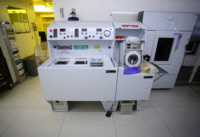
| Model | Semifab WPS-400 |
| Specialist | Paul Tierney (Daniel A. Adams) |
| Physical Location | 2F 2-South DepAndEtch |
Classification
| Process Category | Wet |
| Subcategory | Acids |
| Material Keywords | Photoresist, EBL Resist, Acids |
| Sample Size | 6" Wafers, 4" Wafers |
| Alternative | TRL / acidhood |
| Keywords | multi wafer, manual load, both sides of sample, isotropic etch, temperature, manual operation |
Description
The premetal-piranha is an acid wet station with two baths dedicated to wafer cleaning with piranha solution (1:3, H2O2:H2SO4). One bath is dedicated to stripping photoresist and is denoted with a sign and yellow labware; the second bath is dedicated to pre-deposition cleaning of wafers providing both organic and ionic contamination removal and is denoted with a sign and green labware. A third bath holds a standing solution of 50:1, DI water:HF, and this bath is used in conjunction with the pre-deposition cleaning bath. Each bath has a dedicated timer and quick-dump rinser. The premetal-piranha station shares a spin-rinse dryer with the other acid wet stations in ICL.
| Best for | Removing photoresist and metal ion contaminants prior to metal deposistion. |
| Limitations | Wafers only. Not for etching, only for cleaning. |
| Characteristics/FOM | Piranha solution consists of a 1:3 mix of hydrogen peroxide and sulfuric acid. A typical cleaning process is about 10 minutes, and it is followed by a 1 minute 50:1 water/HF dip (this step is optional) |
| Caution with | Do not process samples that contain exposed metal films, due to aggressive reaction of PIRANHA and metals. Review safety regulations and wear personal protective equipment. |
| Machine Charges | 25/tank |
Documents
SOP
| Piranha | SOP for the ICL piranha baths |
| Wet Processing | Rules and guidelines for wet processing |
Documents
| Etch rates part 2 | Berkeley etch rate paper |
Process Matrix Details
Permitted
Germanium on surfaceSamples with germanium on the surface (typically grown films)
, Germanium buriedSamples with germanium buried below a different film
, Been in the STS DRIEThe DRIE etch leaves behind polymer residues on the sidewall ripples, which can be a contamination concern for some tools.
, Been in the SEMA sample viewed in the SEM must have used the appropriate chuck to avoid cross-contamination
, Been in the Concept1The Concep1 deposits dielectrics on GREEN wafers, however it also accepts metal and there can be cross-contamination for diffusion area
, Has PhotoresistSamples with photoresist cannot be exposed to high temperatures, which is typical in deposition tools. Outgassing can be a concern.
(Removes), Has PolyimidePolyimide is a very chemically resistant polymer, and can tolerate higher temperatures but cannot be exposed to typical PECVD deposition temperatures or diffusion furnaces. Outgassing can be a concern.
(Removes), Coming from KOHAfter a KOH etch, the samples must receive a special clean because the K ions are highly contaminating to CMOS frontend tools
(Removes), Coming from CMPAfter a CMP, the samples must receive a special clean, because the slurry residues otherwise introduce contamination and particles.
(Removes)
Not Allowed
Ever been in EMLSamples from EML are never permitted to return to ICL or TRL
, Been in the ALDSamples that have been in any of the ALD systems
, Pyrex SubstratesPyrex substrates can be a concern due to high sodium content, which contaminates CMOS frontend tools
, III-V SubstratesAny III-V substrates, e.g. GaAs, GaN, InP, and so on. Note though that many common III-V substrates will also carry the Au flag, but there are some GREEN III-V substrates.
, PiecesWafer pieces may not be handled by the equipment, and are harder to thoroughly clean - preventing them from running in certain tools.
, Gold or RED color codeRED color code substrates. These are gold-contaminated or have been processed in gold contaminated tools. Gold and other metals can contaminate silicon devices (GREEN color code) and have to be separated.
, Any exposure to CMOS metalIf the sample had ever seen a CMOS metal (or a tool that accepts CMOS metal), then some frontend tools could be contaminated by this.
, CMOS metal on surfaceCMOS compatible metals exposed on the surface. These are Al,Ni,Pt,Ti,TiN. Other metals such as Au are *NOT* part of this.
, CMOS metal buriedCMOS compatible metals covered entirely by a different material. These are Al,Ni,Pt,Ti,TiN. Other metals such as Au are *NOT* part of this.
, Has Cured SU8Not fully cured SU8 residues can heavily contaminated plasma chambers or destroy other user's samples, but fully cured SU8 is permitted in certain tools.
For more details or help, please consult PTC matrix, email ptc@mtl.mit.edu, or ask the research specialist (Paul Tierney)