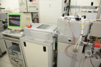
Equipment
| Lab and Coral Name | TRL / sts2 |
| Model | STS/Multiplex ICP MESC |
| Specialist | Donal Jamieson (Dennis Ward) |
| Physical Location | 4F Main-South |
Classification
| Process Category | Etch |
| Subcategory | DRIE |
| Material Keywords | Silicon, SiNx |
| Sample Size | 6" Wafers, Pieces Require Puck |
| Alternative | ICL / AME, TRL / STS1 |
| Keywords | single wafer, load lock, top side of sample, anisotropic etch, vacuum, plasma |
Description
The sts2 is a Deep Reactive Ion Etcher (DRIE) with RF generated, inductively coupled plasma. It is designed for high aspect ration silicon trench etching and deep/through wafer anisotropic etching. The tool uses the Bosch process of time multiplexed deep etching (TMDE) to achieve high aspect ratio etches. This process utilises an etch cycle flowing only SF6 and then switching to a sidewall passivation cycle using only C4F8. During the subsequent etch cycle, the passivating film is preferentially removed from the bottom of the trenches using ion bombardment. High etch-rate isotropic silicon etching is also possible, but not for bulk removal. The tool can also be used for etching silicon nitride. The load-lock has a dual-wafer carousel.
| Best for | high aspect silicon trenches, through wafer etching |
| Limitations | Not intended for bulk removal of silicon (e.g. wafer thinning). Nitride etch has poor selectivity to silicon. |
| Characteristics/FOM | Available gases: C4H8, SF6, O2; Good selectivity to oxide and photoresist masks. Etch rates around 1-2 um/min, depending on recipe. |
| Caution with | when etching through-wafer trenches, the wafer can break. It must be mounted on a 6" carrier wafer. Pieces and 4" wafers also need to be mounted on a carrier wafer. |
| Machine Charges | 7/wafer + 0.04/um |
Documents
SOP
| DRIE | SOP for the 2st generation STS DRIE |
| Kapton Tape | SOP for the use of Kapton tape in the DRIE etchers |
Documents
| Etch rates part 2 | Berkeley etch rate paper |
| Etch rates part 1 | Berkeley etch rate paper |
External Links
| Dry Etching for VLSI | Fundamentals of dry etching, good introduction text |
Process Matrix Details
Permitted
PiecesWafer pieces may not be handled by the equipment, and are harder to thoroughly clean - preventing them from running in certain tools.
, Any exposure to CMOS metalIf the sample had ever seen a CMOS metal (or a tool that accepts CMOS metal), then some frontend tools could be contaminated by this.
, CMOS metal buriedCMOS compatible metals covered entirely by a different material. These are Al,Ni,Pt,Ti,TiN. Other metals such as Au are *NOT* part of this.
, Been in the STS DRIEThe DRIE etch leaves behind polymer residues on the sidewall ripples, which can be a contamination concern for some tools.
(Adds), Been in the SEMA sample viewed in the SEM must have used the appropriate chuck to avoid cross-contamination
, Been in the Concept1The Concep1 deposits dielectrics on GREEN wafers, however it also accepts metal and there can be cross-contamination for diffusion area
, Has PhotoresistSamples with photoresist cannot be exposed to high temperatures, which is typical in deposition tools. Outgassing can be a concern.
, Coming from KOHAfter a KOH etch, the samples must receive a special clean because the K ions are highly contaminating to CMOS frontend tools
, Coming from CMPAfter a CMP, the samples must receive a special clean, because the slurry residues otherwise introduce contamination and particles.
Not Allowed
Ever been in EMLSamples from EML are never permitted to return to ICL or TRL
, Been in the ALDSamples that have been in any of the ALD systems
, Pyrex SubstratesPyrex substrates can be a concern due to high sodium content, which contaminates CMOS frontend tools
, III-V SubstratesAny III-V substrates, e.g. GaAs, GaN, InP, and so on. Note though that many common III-V substrates will also carry the Au flag, but there are some GREEN III-V substrates.
, Germanium on surfaceSamples with germanium on the surface (typically grown films)
, Germanium buriedSamples with germanium buried below a different film
, Gold or RED color codeRED color code substrates. These are gold-contaminated or have been processed in gold contaminated tools. Gold and other metals can contaminate silicon devices (GREEN color code) and have to be separated.
, CMOS metal on surfaceCMOS compatible metals exposed on the surface. These are Al,Ni,Pt,Ti,TiN. Other metals such as Au are *NOT* part of this.
, Has PolyimidePolyimide is a very chemically resistant polymer, and can tolerate higher temperatures but cannot be exposed to typical PECVD deposition temperatures or diffusion furnaces. Outgassing can be a concern.
, Has Cured SU8Not fully cured SU8 residues can heavily contaminated plasma chambers or destroy other user's samples, but fully cured SU8 is permitted in certain tools.
For more details or help, please consult PTC matrix, email ptc@mtl.mit.edu, or ask the research specialist (Donal Jamieson)