Equipment
| Lab and Coral Name | TRL / EV1 |
| Model | Electronic Visions 620 |
| Specialist | David Terry (Paul Tierney) |
| Physical Location | 4F Photo-North |
Classification
| Process Category | Photo |
| Subcategory | Expose |
| Material Keywords | Polyimide, SU8, Photoresist |
| Sample Size | 6" Wafers, 4" Wafers, Pieces |
| Alternative | TRL / EV-LC |
| Keywords | single wafer, manual load, top side of sample, manual operation, alignment |
Description
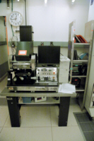
The EV1 is a mask aligner for contact alignment between a photomask and a wafer, capable of front- and back-side alignment. The tool exposes with 365-405 nm UV light with constant intensity, and the user sets the exposure time to adjust the dose. It has hard- and soft-contact modes. The tool has front-side and back-side alignment capability. Alignment on darkfield masks can be difficult, and proper alignment mark design is important to allow sufficient open space to view the wafer during alignment. This tool is similar to the EV-LC, with minor design differences in the mask holder and cameras.
| Best for | Contact alignment with feature sizes above 1-3um depending on the pattern. Exposing SU8 (with correct chucks) |
| Limitations | Feature sizes below 2-3 um may require careful exposure time and/or pattern optimization. UV intensity is not perfectly uniform, and will also change over the lamp life. |
| Characteristics/FOM | 365-405 nm |
| Caution with | The EV1 is not ideal for pieces, and can crush them. If using pieces, place dummies around your sample to balance the pressure, or use the MA-6 instead. Thick resist may be best exposed in intervals to avoid bubbling. Park the tool when done, to avoid software issues for the next user. Placing underbaked photoresist into the tool will get the wafers stuck to your mask. When processing SU8, use separate SU8 labware. |
| Machine Charges | 6/wafer |
Documents
SOP
| EV1 | SOP for the EV1 mask aligner |
| Resist Recipes | Baseline resist recipes for TRL |
External Links
| Guide | MicroChem Application Notes |
Process Matrix Details
Permitted
Been in the ALDSamples that have been in any of the ALD systems
, Pyrex SubstratesPyrex substrates can be a concern due to high sodium content, which contaminates CMOS frontend tools
, III-V SubstratesAny III-V substrates, e.g. GaAs, GaN, InP, and so on. Note though that many common III-V substrates will also carry the Au flag, but there are some GREEN III-V substrates.
, Germanium on surfaceSamples with germanium on the surface (typically grown films)
, Germanium buriedSamples with germanium buried below a different film
, PiecesWafer pieces may not be handled by the equipment, and are harder to thoroughly clean - preventing them from running in certain tools.
, Gold or RED color codeRED color code substrates. These are gold-contaminated or have been processed in gold contaminated tools. Gold and other metals can contaminate silicon devices (GREEN color code) and have to be separated.
, Any exposure to CMOS metalIf the sample had ever seen a CMOS metal (or a tool that accepts CMOS metal), then some frontend tools could be contaminated by this.
, CMOS metal on surfaceCMOS compatible metals exposed on the surface. These are Al,Ni,Pt,Ti,TiN. Other metals such as Au are *NOT* part of this.
, CMOS metal buriedCMOS compatible metals covered entirely by a different material. These are Al,Ni,Pt,Ti,TiN. Other metals such as Au are *NOT* part of this.
, Been in the STS DRIEThe DRIE etch leaves behind polymer residues on the sidewall ripples, which can be a contamination concern for some tools.
, Been in the SEMA sample viewed in the SEM must have used the appropriate chuck to avoid cross-contamination
, Been in the Concept1The Concep1 deposits dielectrics on GREEN wafers, however it also accepts metal and there can be cross-contamination for diffusion area
, Has PhotoresistSamples with photoresist cannot be exposed to high temperatures, which is typical in deposition tools. Outgassing can be a concern.
, Has PolyimidePolyimide is a very chemically resistant polymer, and can tolerate higher temperatures but cannot be exposed to typical PECVD deposition temperatures or diffusion furnaces. Outgassing can be a concern.
, Has Cured SU8Not fully cured SU8 residues can heavily contaminated plasma chambers or destroy other user's samples, but fully cured SU8 is permitted in certain tools.
, Coming from KOHAfter a KOH etch, the samples must receive a special clean because the K ions are highly contaminating to CMOS frontend tools
, Coming from CMPAfter a CMP, the samples must receive a special clean, because the slurry residues otherwise introduce contamination and particles.
Not Allowed
Ever been in EMLSamples from EML are never permitted to return to ICL or TRL
For more details or help, please consult PTC matrix, email ptc@mtl.mit.edu, or ask the research specialist (David Terry)