Equipment
| Lab and Coral Name | TRL / Heidelberg |
| Model | Heidelberg DWL-66 |
| Specialist | Dennis Ward (Paul Tierney) |
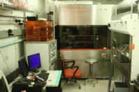
| Physical Location | 4F External-Photo |
Classification
| Process Category | Photo |
| Subcategory | Expose |
| Material Keywords | Photoresist |
| Sample Size | 8" Wafers, 6" Wafers, 4" Wafers, 7" Photo Plates, 5" Photo Plates, Pieces |
| Alternative | None |
| Keywords | single wafer, manual load, top side of sample, manual operation, alignment |
Description
The Heidelberg is a direct-write laser system that can expose UV sensitive photoresist on wafers or masks, using a 405nm diode laser. The system has interchangeable write heads that trade off speed for feature size. Typically, the 20mm head is used for features of 4-5um or greater, while the 10mm head is used for when features are between 2 and 4 um. Additionally, the 4mm head can expose to approximately 1um resolution. However, at these dimensions careful calibration of exposure conditons and patterns will be required. While the most common use is for in-house mask writing, directly exposing resist coated wafers is a core strength of this tool and the system contains a CCD camera with pattern recognition software for accurate alignment to existing layers on a wafer. The tool is also capable of grayscale lithography. A full 6" wafer takes 3-4 hours with the 20mm head, and 9-12 hours with the 10mm head. The 4mm head is not practical for full wafers and 7" mask plates, but can be used for 5" mask plates, pieces/dies or 4" wafers.
| Best for | Mask writing, aligned direct write on wafers or pieces, grayscale lithography |
| Limitations | Writing a large number of wafers is not practical. There are differences in pattern direction due to field stitching. Wafers with large topology (e.g. MEMS devices) can be challenging. |
| Characteristics/FOM | 405 nm diode laser |
| Caution with | Do not touch or bump into the objective, this can cause damage. Similarly, be careful when focusing to make sure the focus is done on the sample, otherwise you risk crashing the objective into the sample. |
| Machine Charges | 10/hour |
Documents
SOP
| Direct-Write Laser System | SOP for the DWL66 direct laser writer |
| Resist Recipes | Baseline resist recipes for TRL |
External Links
| Guide | MicroChem Application Notes |
Process Matrix Details
Permitted
Been in the ALDSamples that have been in any of the ALD systems
, Pyrex SubstratesPyrex substrates can be a concern due to high sodium content, which contaminates CMOS frontend tools
, III-V SubstratesAny III-V substrates, e.g. GaAs, GaN, InP, and so on. Note though that many common III-V substrates will also carry the Au flag, but there are some GREEN III-V substrates.
, Germanium on surfaceSamples with germanium on the surface (typically grown films)
, Germanium buriedSamples with germanium buried below a different film
, PiecesWafer pieces may not be handled by the equipment, and are harder to thoroughly clean - preventing them from running in certain tools.
, Gold or RED color codeRED color code substrates. These are gold-contaminated or have been processed in gold contaminated tools. Gold and other metals can contaminate silicon devices (GREEN color code) and have to be separated.
, Any exposure to CMOS metalIf the sample had ever seen a CMOS metal (or a tool that accepts CMOS metal), then some frontend tools could be contaminated by this.
, CMOS metal on surfaceCMOS compatible metals exposed on the surface. These are Al,Ni,Pt,Ti,TiN. Other metals such as Au are *NOT* part of this.
, CMOS metal buriedCMOS compatible metals covered entirely by a different material. These are Al,Ni,Pt,Ti,TiN. Other metals such as Au are *NOT* part of this.
, Been in the STS DRIEThe DRIE etch leaves behind polymer residues on the sidewall ripples, which can be a contamination concern for some tools.
, Been in the SEMA sample viewed in the SEM must have used the appropriate chuck to avoid cross-contamination
, Been in the Concept1The Concep1 deposits dielectrics on GREEN wafers, however it also accepts metal and there can be cross-contamination for diffusion area
, Has PhotoresistSamples with photoresist cannot be exposed to high temperatures, which is typical in deposition tools. Outgassing can be a concern.
, Has PolyimidePolyimide is a very chemically resistant polymer, and can tolerate higher temperatures but cannot be exposed to typical PECVD deposition temperatures or diffusion furnaces. Outgassing can be a concern.
, Has Cured SU8Not fully cured SU8 residues can heavily contaminated plasma chambers or destroy other user's samples, but fully cured SU8 is permitted in certain tools.
, Coming from KOHAfter a KOH etch, the samples must receive a special clean because the K ions are highly contaminating to CMOS frontend tools
, Coming from CMPAfter a CMP, the samples must receive a special clean, because the slurry residues otherwise introduce contamination and particles.
Not Allowed
Ever been in EMLSamples from EML are never permitted to return to ICL or TRL
For more details or help, please consult PTC matrix, email ptc@mtl.mit.edu, or ask the research specialist (Dennis Ward )