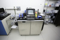
Equipment
| Lab and Coral Name | ICL / LAM490B |
| Model | LAM 490B |
| Specialist | Robert Bicchieri (Eric Lim) |
| Physical Location | 2F 2-North Etch |
Classification
| Process Category | Etch |
| Subcategory | RIE |
| Material Keywords | Silicon, SiO2, SiNx, Dielectrics |
| Sample Size | 6" Wafers, Pieces Require Puck |
| Alternative | ICL / AME-5000 |
| Keywords | multi wafer, load lock, top side of sample, anisotropic etch, vacuum, plasma |
Description
The LAM490B is a parallel plate plasma etcher with RF generated plasma. It has a single chamber that allows for etching of silicon using chlorine chemistry and silicon nitride using fluorine chemistry; if switching from one chemistry to the other, the chamber requires conditioning with several dummy wafers. Standard etch recipes are loaded into the tool via data cartridges and can be edited in the tool memory. This tool serves as the backup front end etcher and accepts GREEN samples.
| Best for | Silicon and nitride etching |
| Limitations | Poor selectivities for Si:PR (1.6:1) and SiN:Si |
| Characteristics/FOM | Approximate etch rates: Si etch is 55 A/sec, Si3N4 etch is 17 A/sec. Etch gases: C2F6, SF6, Cl2, He, O2 |
| Caution with | Deep Si etching requires an oxide mask and cool-down times. Mounting of wafers onto a handle wafer can result in excess heating, resist burning, or dismounting of the handle wafer. |
| Machine Charges | 7/wafer + 1/um |
Documents
SOP
| LAM490B | SOP for the LAM490B etcher |
Documents
| Etch rates part 2 | Berkeley etch rate paper |
| Etch rates part 1 | Berkeley etch rate paper |
External Links
| Dry Etching for VLSI | Fundamentals of dry etching, good introduction text |
Process Matrix Details
Permitted
Germanium on surfaceSamples with germanium on the surface (typically grown films)
, Germanium buriedSamples with germanium buried below a different film
, PiecesWafer pieces may not be handled by the equipment, and are harder to thoroughly clean - preventing them from running in certain tools.
, Any exposure to CMOS metalIf the sample had ever seen a CMOS metal (or a tool that accepts CMOS metal), then some frontend tools could be contaminated by this.
, CMOS metal buriedCMOS compatible metals covered entirely by a different material. These are Al,Ni,Pt,Ti,TiN. Other metals such as Au are *NOT* part of this.
, Been in the STS DRIEThe DRIE etch leaves behind polymer residues on the sidewall ripples, which can be a contamination concern for some tools.
, Been in the SEMA sample viewed in the SEM must have used the appropriate chuck to avoid cross-contamination
(With Appropriate Chuck), Been in the Concept1The Concep1 deposits dielectrics on GREEN wafers, however it also accepts metal and there can be cross-contamination for diffusion area
, Has PhotoresistSamples with photoresist cannot be exposed to high temperatures, which is typical in deposition tools. Outgassing can be a concern.
, Has PolyimidePolyimide is a very chemically resistant polymer, and can tolerate higher temperatures but cannot be exposed to typical PECVD deposition temperatures or diffusion furnaces. Outgassing can be a concern.
, Coming from KOHAfter a KOH etch, the samples must receive a special clean because the K ions are highly contaminating to CMOS frontend tools
, Coming from CMPAfter a CMP, the samples must receive a special clean, because the slurry residues otherwise introduce contamination and particles.
Not Allowed
Ever been in EMLSamples from EML are never permitted to return to ICL or TRL
, Been in the ALDSamples that have been in any of the ALD systems
, Pyrex SubstratesPyrex substrates can be a concern due to high sodium content, which contaminates CMOS frontend tools
, III-V SubstratesAny III-V substrates, e.g. GaAs, GaN, InP, and so on. Note though that many common III-V substrates will also carry the Au flag, but there are some GREEN III-V substrates.
, Gold or RED color codeRED color code substrates. These are gold-contaminated or have been processed in gold contaminated tools. Gold and other metals can contaminate silicon devices (GREEN color code) and have to be separated.
, CMOS metal on surfaceCMOS compatible metals exposed on the surface. These are Al,Ni,Pt,Ti,TiN. Other metals such as Au are *NOT* part of this.
, Has Cured SU8Not fully cured SU8 residues can heavily contaminated plasma chambers or destroy other user's samples, but fully cured SU8 is permitted in certain tools.
For more details or help, please consult PTC matrix, email ptc@mtl.mit.edu, or ask the research specialist (Robert Bicchieri)