Equipment
| Lab and Coral Name | ICL / LAM590-ICL |
| Model | LAM 590B |
| Specialist | Robert Bicchieri (Eric Lim) |
| Physical Location | 2F 2-North Etch |
Classification
| Process Category | Etch |
| Subcategory | RIE |
| Material Keywords | SiO2, SiNx, Dielectrics |
| Sample Size | 6" Wafers, Pieces Require Puck |
| Alternative | ICL / AME5000 |
| Keywords | multi wafer, load lock, top side of sample, anisotropic etch, vacuum, plasma |
Description
The LAM590 is a reactive ion etcher with RF generated plasma. It is a single chamber system designed for etching silicon oxides with fluorine chemistry, and it can also etch silicon nitride. It can process wafers with CMOS metal present, which makes it the ideal choice for backend processing (for example etching contacts through oxide to open metal pads). The LAM590-TRL is an identical tool but designated for RED processes. Standard photoresist as well as PMMA can be used as masks.
| Best for | Dielectric etching when CMOS metal is present on wafer |
| Limitations | Pieces and smaller wafers require a handle wafer, and improper mounting can result in resist burning and other problems |
| Characteristics/FOM | CF4, CHF3, He, O2, RF power up to 1200W, single wafer, cassette |
| Caution with | Thick resist can bubble up if not properly hard-baked. Mounting of wafers onto a handle wafer can result in excess heating, resist burning, or dismounting of the handle wafer. |
| Machine Charges | 7/wafer + 1/um |
Documents
SOP
| LAM590 | SOP for the LAM590 etcher |
Recipes
| Oxide Etching | Baseline oxide etch recipes for the LAM590 |
Documents
| Etch rates part 2 | Berkeley etch rate paper |
| Etch rates part 1 | Berkeley etch rate paper |
Images
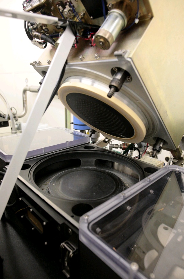
| Etch Chamber | Photo of the LAM590 etch chamber when opened |
External Links
| Dry Etching for VLSI | Fundamentals of dry etching, good introduction text |
Process Matrix Details
Permitted
Been in the ALDSamples that have been in any of the ALD systems
, Germanium on surfaceSamples with germanium on the surface (typically grown films)
, Germanium buriedSamples with germanium buried below a different film
, PiecesWafer pieces may not be handled by the equipment, and are harder to thoroughly clean - preventing them from running in certain tools.
, Any exposure to CMOS metalIf the sample had ever seen a CMOS metal (or a tool that accepts CMOS metal), then some frontend tools could be contaminated by this.
, CMOS metal on surfaceCMOS compatible metals exposed on the surface. These are Al,Ni,Pt,Ti,TiN. Other metals such as Au are *NOT* part of this.
, CMOS metal buriedCMOS compatible metals covered entirely by a different material. These are Al,Ni,Pt,Ti,TiN. Other metals such as Au are *NOT* part of this.
, Been in the STS DRIEThe DRIE etch leaves behind polymer residues on the sidewall ripples, which can be a contamination concern for some tools.
, Been in the SEMA sample viewed in the SEM must have used the appropriate chuck to avoid cross-contamination
(With Appropriate Chuck), Been in the Concept1The Concep1 deposits dielectrics on GREEN wafers, however it also accepts metal and there can be cross-contamination for diffusion area
, Has PhotoresistSamples with photoresist cannot be exposed to high temperatures, which is typical in deposition tools. Outgassing can be a concern.
, Has PolyimidePolyimide is a very chemically resistant polymer, and can tolerate higher temperatures but cannot be exposed to typical PECVD deposition temperatures or diffusion furnaces. Outgassing can be a concern.
, Coming from KOHAfter a KOH etch, the samples must receive a special clean because the K ions are highly contaminating to CMOS frontend tools
, Coming from CMPAfter a CMP, the samples must receive a special clean, because the slurry residues otherwise introduce contamination and particles.
Not Allowed
Ever been in EMLSamples from EML are never permitted to return to ICL or TRL
, Pyrex SubstratesPyrex substrates can be a concern due to high sodium content, which contaminates CMOS frontend tools
, III-V SubstratesAny III-V substrates, e.g. GaAs, GaN, InP, and so on. Note though that many common III-V substrates will also carry the Au flag, but there are some GREEN III-V substrates.
, Gold or RED color codeRED color code substrates. These are gold-contaminated or have been processed in gold contaminated tools. Gold and other metals can contaminate silicon devices (GREEN color code) and have to be separated.
, Has Cured SU8Not fully cured SU8 residues can heavily contaminated plasma chambers or destroy other user's samples, but fully cured SU8 is permitted in certain tools.
For more details or help, please consult PTC matrix, email ptc@mtl.mit.edu, or ask the research specialist (Robert Bicchieri)