Equipment
| Lab and Coral Name | ICL / diesaw |
| Model | Disco DAD-2H/6T |
| Specialist | Timothy Turner (Ryan O'Keefe) |
| Physical Location | 5F 3-South Packaging |
Classification
| Process Category | Packaging |
| Subcategory | Physical |
| Material Keywords | Silicon, III-V, GaN, Quartz, Pyrex |
| Sample Size | 6" Wafers, 4" Wafers, Pieces |
| Alternative | WaferCleaving |
| Keywords | single wafer, manual load, top side of sample, manual operation, alignment |
Description
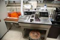
The diesaw is a sawing tool for cutting wafers into smaller pieces, and is typically used at the conclusion of a process. Wafers are attached to UV-release tape, and the saw can make a number of periodic cuts aligned to the dies on the wafer. Different blades exist for various materials (e.g. Si, pyrex, etc). The tape can be released by placing it into the UV exposure system next to the diesaw.
| Best for | Cutting completed wafers into regular and precisely shaped dies that are aligned to existing patterns (in comparison to cleaving) for testing and packaging. |
| Limitations | The diesaw can also be used to create small dies from a new wafer as starting material for processing. However, diesawing will result in a lot of dirt, and more elaborate cleaning will be required if diced wafers are to be processed in TRL - in contrast to cleaving wafers. See Procedures-Cleaning for more details. |
| Characteristics/FOM | There are two available blades for cutting silicon (32 um and 200 um thick) and one blade for cutting glass (pyrex) which is 240 um thick. |
| Caution with | If wafer top-side has fragile features, a photoresist coat can help to protect it from contamination during dicing. For certain III-V wafer dicing, be aware of safety issues and that III-V dust may present. See MTL Safety Officer with questions for specific situations. Ensure proper tape adhesion to prevent dies from coming off during process. Adjusting cut depth can help with very small dies. |
| Machine Charges | 3/wafer + 0.1/cut |
Documents
Process Matrix Details
Permitted
Been in the ALDSamples that have been in any of the ALD systems
, Pyrex SubstratesPyrex substrates can be a concern due to high sodium content, which contaminates CMOS frontend tools
, III-V SubstratesAny III-V substrates, e.g. GaAs, GaN, InP, and so on. Note though that many common III-V substrates will also carry the Au flag, but there are some GREEN III-V substrates.
, Germanium on surfaceSamples with germanium on the surface (typically grown films)
, Germanium buriedSamples with germanium buried below a different film
, PiecesWafer pieces may not be handled by the equipment, and are harder to thoroughly clean - preventing them from running in certain tools.
, Gold or RED color codeRED color code substrates. These are gold-contaminated or have been processed in gold contaminated tools. Gold and other metals can contaminate silicon devices (GREEN color code) and have to be separated.
(Adds), Any exposure to CMOS metalIf the sample had ever seen a CMOS metal (or a tool that accepts CMOS metal), then some frontend tools could be contaminated by this.
, CMOS metal on surfaceCMOS compatible metals exposed on the surface. These are Al,Ni,Pt,Ti,TiN. Other metals such as Au are *NOT* part of this.
, CMOS metal buriedCMOS compatible metals covered entirely by a different material. These are Al,Ni,Pt,Ti,TiN. Other metals such as Au are *NOT* part of this.
, Been in the STS DRIEThe DRIE etch leaves behind polymer residues on the sidewall ripples, which can be a contamination concern for some tools.
, Been in the SEMA sample viewed in the SEM must have used the appropriate chuck to avoid cross-contamination
, Been in the Concept1The Concep1 deposits dielectrics on GREEN wafers, however it also accepts metal and there can be cross-contamination for diffusion area
, Has PhotoresistSamples with photoresist cannot be exposed to high temperatures, which is typical in deposition tools. Outgassing can be a concern.
, Has PolyimidePolyimide is a very chemically resistant polymer, and can tolerate higher temperatures but cannot be exposed to typical PECVD deposition temperatures or diffusion furnaces. Outgassing can be a concern.
, Has Cured SU8Not fully cured SU8 residues can heavily contaminated plasma chambers or destroy other user's samples, but fully cured SU8 is permitted in certain tools.
, Coming from KOHAfter a KOH etch, the samples must receive a special clean because the K ions are highly contaminating to CMOS frontend tools
, Coming from CMPAfter a CMP, the samples must receive a special clean, because the slurry residues otherwise introduce contamination and particles.
Not Allowed
Ever been in EMLSamples from EML are never permitted to return to ICL or TRL
For more details or help, please consult PTC matrix, email ptc@mtl.mit.edu, or ask the research specialist (Timothy Turner)