Equipment
| Lab and Coral Name | ICL / goldwire |
| Model | MEI |
| Specialist | Timothy Turner (Ryan O'Keefe) |
| Physical Location | 5F 3-South Packaging |
Classification
| Process Category | Packaging |
| Subcategory | Physical |
| Material Keywords | CMOS Metals, Non-CMOS Metals |
| Sample Size | 6" Wafers, 4" Wafers, Pieces |
| Alternative | None |
| Keywords | manual load, multiple pieces, top side of sample, temperature, manual operation, alignment |
Description
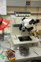
The wirebonder is used to connect metal pads from a chip to a package or circuit board. The bonder uses a gold wire and ultrasonic welding to form a metallurgic connection. Typical pad metals are aluminum or gold. Aluminum pads can have problems with Au-Al intermetallics, gold may be preferred. The system is capable of heating the chuck, which can be useful for some applications.
| Best for | Wirebonding of gold metal pads from a die to a package or a PCBs with ENIG finish |
| Limitations | Pads should be 75um in size or larger to make it easier to bond (smaller is possible but more challenging). Low power settings can result in lack of bonding, and high power settings can result in pad damage and short circuits, or bond failure. These parameters depend on the pad material stack. |
| Characteristics/FOM | |
| Caution with | Pad surfaces must be clean, or bonding can fail. Adjusting the height accurately and making sure the chip is properly secured (no give when pressing down on it) are critical requirements for a successful bonding, particularly when bonding to a PCB. |
| Machine Charges | 7/hour |
Documents
SOP
| Wirebonder | SOP for the gold wirebonder |
Process Matrix Details
Permitted
Been in the ALDSamples that have been in any of the ALD systems
, Pyrex SubstratesPyrex substrates can be a concern due to high sodium content, which contaminates CMOS frontend tools
, III-V SubstratesAny III-V substrates, e.g. GaAs, GaN, InP, and so on. Note though that many common III-V substrates will also carry the Au flag, but there are some GREEN III-V substrates.
, Germanium on surfaceSamples with germanium on the surface (typically grown films)
, Germanium buriedSamples with germanium buried below a different film
, PiecesWafer pieces may not be handled by the equipment, and are harder to thoroughly clean - preventing them from running in certain tools.
, Gold or RED color codeRED color code substrates. These are gold-contaminated or have been processed in gold contaminated tools. Gold and other metals can contaminate silicon devices (GREEN color code) and have to be separated.
(Adds), Any exposure to CMOS metalIf the sample had ever seen a CMOS metal (or a tool that accepts CMOS metal), then some frontend tools could be contaminated by this.
, CMOS metal on surfaceCMOS compatible metals exposed on the surface. These are Al,Ni,Pt,Ti,TiN. Other metals such as Au are *NOT* part of this.
, CMOS metal buriedCMOS compatible metals covered entirely by a different material. These are Al,Ni,Pt,Ti,TiN. Other metals such as Au are *NOT* part of this.
, Been in the STS DRIEThe DRIE etch leaves behind polymer residues on the sidewall ripples, which can be a contamination concern for some tools.
, Been in the SEMA sample viewed in the SEM must have used the appropriate chuck to avoid cross-contamination
, Been in the Concept1The Concep1 deposits dielectrics on GREEN wafers, however it also accepts metal and there can be cross-contamination for diffusion area
, Has PhotoresistSamples with photoresist cannot be exposed to high temperatures, which is typical in deposition tools. Outgassing can be a concern.
, Has PolyimidePolyimide is a very chemically resistant polymer, and can tolerate higher temperatures but cannot be exposed to typical PECVD deposition temperatures or diffusion furnaces. Outgassing can be a concern.
, Has Cured SU8Not fully cured SU8 residues can heavily contaminated plasma chambers or destroy other user's samples, but fully cured SU8 is permitted in certain tools.
, Coming from KOHAfter a KOH etch, the samples must receive a special clean because the K ions are highly contaminating to CMOS frontend tools
, Coming from CMPAfter a CMP, the samples must receive a special clean, because the slurry residues otherwise introduce contamination and particles.
Not Allowed
Ever been in EMLSamples from EML are never permitted to return to ICL or TRL
For more details or help, please consult PTC matrix, email ptc@mtl.mit.edu, or ask the research specialist (Timothy Turner)