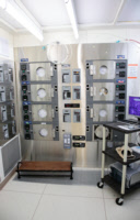
Equipment
| Lab and Coral Name | TRL / A3-Sinter |
| Model | MRL 718 |
| Specialist | Bernard Alamariu (Eric Lim) |
| Physical Location | 4F Entry Diffusion |
Classification
| Process Category | Diffusion |
| Subcategory | Bake |
| Material Keywords | SiO2, SiNx, Dielectrics, CMOS Metals, Non-CMOS Metals |
| Sample Size | 6" Wafers, 4" Wafers |
| Alternative | ICL / RTA2 |
| Keywords | multi wafer, manual load, multiple pieces, both sides of sample, conformal dep, temperature, manual operation |
Description
A3-Sinter is an atmospheric furnace designed to sinter CMOS metals in the temperature range of 300-600C on Si wafers without any prior non-CMOS metals (e.g. Au) or III-V processing. Multistep process recipes (time and gas flows) can be programmed using the associated Sequencer. The temperature profile is separately adjusted using an Eurotherm controller. Center zone temperature can be set directly. Set points for Load and Source zones must be adjusted relative to the Center zone by the user to achieve a flat temperature profile. Wafers are loaded manually with a boat loader and two rods.
| Best for | CMOS metal sintering |
| Limitations | Relatively lower temperature range, only CMOS metal allowed (no Au or III-V's) |
| Characteristics/FOM | Gases: N2, H2, Ar |
| Caution with | |
| Machine Charges | 25/run + 10/um |
Documents
SOP
| Tube A3 | SOP for the diffusion tube A3 |
Process Matrix Details
Permitted
Been in the ALDSamples that have been in any of the ALD systems
, Germanium on surfaceSamples with germanium on the surface (typically grown films)
, Germanium buriedSamples with germanium buried below a different film
, PiecesWafer pieces may not be handled by the equipment, and are harder to thoroughly clean - preventing them from running in certain tools.
, Any exposure to CMOS metalIf the sample had ever seen a CMOS metal (or a tool that accepts CMOS metal), then some frontend tools could be contaminated by this.
(Adds), CMOS metal on surfaceCMOS compatible metals exposed on the surface. These are Al,Ni,Pt,Ti,TiN. Other metals such as Au are *NOT* part of this.
, CMOS metal buriedCMOS compatible metals covered entirely by a different material. These are Al,Ni,Pt,Ti,TiN. Other metals such as Au are *NOT* part of this.
, Been in the SEMA sample viewed in the SEM must have used the appropriate chuck to avoid cross-contamination
(With Appropriate Chuck), Been in the Concept1The Concep1 deposits dielectrics on GREEN wafers, however it also accepts metal and there can be cross-contamination for diffusion area
, Coming from KOHAfter a KOH etch, the samples must receive a special clean because the K ions are highly contaminating to CMOS frontend tools
, Coming from CMPAfter a CMP, the samples must receive a special clean, because the slurry residues otherwise introduce contamination and particles.
Not Allowed
Ever been in EMLSamples from EML are never permitted to return to ICL or TRL
, Pyrex SubstratesPyrex substrates can be a concern due to high sodium content, which contaminates CMOS frontend tools
, III-V SubstratesAny III-V substrates, e.g. GaAs, GaN, InP, and so on. Note though that many common III-V substrates will also carry the Au flag, but there are some GREEN III-V substrates.
, Gold or RED color codeRED color code substrates. These are gold-contaminated or have been processed in gold contaminated tools. Gold and other metals can contaminate silicon devices (GREEN color code) and have to be separated.
, Been in the STS DRIEThe DRIE etch leaves behind polymer residues on the sidewall ripples, which can be a contamination concern for some tools.
, Has PhotoresistSamples with photoresist cannot be exposed to high temperatures, which is typical in deposition tools. Outgassing can be a concern.
, Has PolyimidePolyimide is a very chemically resistant polymer, and can tolerate higher temperatures but cannot be exposed to typical PECVD deposition temperatures or diffusion furnaces. Outgassing can be a concern.
, Has Cured SU8Not fully cured SU8 residues can heavily contaminated plasma chambers or destroy other user's samples, but fully cured SU8 is permitted in certain tools.
For more details or help, please consult PTC matrix, email ptc@mtl.mit.edu, or ask the research specialist (Bernard Alamariu)