Equipment
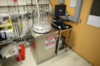
| Lab and Coral Name | EML / ALD-EML |
| Model | Cambridge Nanotech |
| Specialist | Kurt Broderick (Timothy Turner, Gary Riggott) |
| Physical Location | TBD |
Classification
| Process Category | Deposition |
| Subcategory | CVD |
| Material Keywords | Dielectrics, CMOS Metals, Non-Standard Materials |
| Sample Size | 6" Wafers, 4" Wafers, Pieces |
| Alternative | none |
| Keywords | single wafer, manual load, multiple pieces, top side of sample, conformal dep, vacuum, temperature, manual operation |
Description
The ALD is a atomic layer dep tool that deposits Al2O3, HfO2 and WN through thermal-assisted process, for RED processes. The deposition takes place in an atomic layer-by-layer fashion, and thereby allows for atomic-scale control of the film thickness. Thin layers (sub-5 nm) can be very well deposited with extremly good uniformity and conformal coverage at moderatively low temperatures (typically below 300 C). Deposition can be done on materials such as Si, III-V and 2D materials. Proper cleaning of the samples (e.g. RCA, Piranha, nanostrip, O2 plasma, etc) before deposition is required to help maintain the cleaningness of the system. No organics (e.g. photoresists) are allowed in this tool.
| Best for | Gate dielectric layers, very thin films, conformal coverage, uniform deposition for sub-5nm layers. |
| Limitations | Slow deposition rate, relatively thin layers only. Any EML processes using this tool must receive PTC approval (the only EML tool for which this is the case). |
| Characteristics/FOM | Al2O3, HfO2, WN |
| Caution with | Proper sample cleaning is required (the choice of cleaning procedures can vary by samples type depending on what it is able to tolerate), to maintain the cleaningness of the tool since it is critical to a number of applications. No organics (polymers, photoresists, etc) are allowed. |
| Machine Charges | 7/wafer + 120/um |
Documents
SOP
| ALD | SOP for the Cambridge Nano ALD |
Process Matrix Details
PTC Matrix does not apply for EML
Ever been in EMLSamples from EML are never permitted to return to ICL or TRL