Equipment
| Lab and Coral Name | ICL / TMAH-KOHhood |
| Model | fume hood |
| Specialist | Kurt Broderick (Timothy Turner) |
| Physical Location | 5F 2-North |
Classification
| Process Category | Wet |
| Subcategory | Acids |
| Material Keywords | Silicon, Acids |
| Sample Size | 6" Wafers, 4" Wafers, Pieces |
| Alternative | none |
| Keywords | multi wafer, manual load, multiple pieces, both sides of sample, isotropic etch, anisotropic etch, temperature, manual operation |
Description
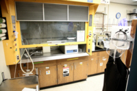
The TMAH-KOH Hood is an acid wet station that has a heated water bath for maintaining temperature of KOH or TMAH chemical solutions. KOH and TMAH chemical baths allow for anisotropic etching of silicon due to varying etch rates along different crystal orientations. This wet station allows for both GREEN and RED processing; KOH processing should be done in YELLOW labware due to the ionic contamination of K+. Post KOH-TMAH cleaning is required for re-entry to ICL/TRL, a double piranha will restore the GREEN state of samples.
| Best for | Anisotropic etching of silicon with high selectivity to oxide and nitride, fast etching, bulk silicon removal |
| Limitations | A hard mask is required (photoresist will not survive the process), and a re-entry clean is required for further processing in ICL/TRL. |
| Characteristics/FOM | KOH etch rate 85+um/hour (80C, 20%), TMAH etch rate 20um/hour (80C, 25%) (but check these numbers) |
| Caution with | TMAH at 25% and 80C is extremely toxic. Wafers may be brittle and fragile after etching. A dilute HF dip may be needed at the start of an etch since even a native oxide can prevent etching. |
| Machine Charges | 25/tank |
Documents
SOP
| TMAH and KOH | SOP for the TMAH and KOH wet station |
| Wet Processing | Rules and guidelines for wet processing |
Documents
| Anisotropic Etching | One of the earlier papers on anisotropic etching of silicon |
| Etch rates part 2 | Berkeley etch rate paper |
Process Matrix Details
Permitted
Been in the ALDSamples that have been in any of the ALD systems
, Germanium on surfaceSamples with germanium on the surface (typically grown films)
, Germanium buriedSamples with germanium buried below a different film
, PiecesWafer pieces may not be handled by the equipment, and are harder to thoroughly clean - preventing them from running in certain tools.
, Gold or RED color codeRED color code substrates. These are gold-contaminated or have been processed in gold contaminated tools. Gold and other metals can contaminate silicon devices (GREEN color code) and have to be separated.
, Any exposure to CMOS metalIf the sample had ever seen a CMOS metal (or a tool that accepts CMOS metal), then some frontend tools could be contaminated by this.
, Been in the STS DRIEThe DRIE etch leaves behind polymer residues on the sidewall ripples, which can be a contamination concern for some tools.
, Been in the SEMA sample viewed in the SEM must have used the appropriate chuck to avoid cross-contamination
, Been in the Concept1The Concep1 deposits dielectrics on GREEN wafers, however it also accepts metal and there can be cross-contamination for diffusion area
, Has PhotoresistSamples with photoresist cannot be exposed to high temperatures, which is typical in deposition tools. Outgassing can be a concern.
, Has PolyimidePolyimide is a very chemically resistant polymer, and can tolerate higher temperatures but cannot be exposed to typical PECVD deposition temperatures or diffusion furnaces. Outgassing can be a concern.
, Coming from KOHAfter a KOH etch, the samples must receive a special clean because the K ions are highly contaminating to CMOS frontend tools
(Adds), Coming from CMPAfter a CMP, the samples must receive a special clean, because the slurry residues otherwise introduce contamination and particles.
Not Allowed
Ever been in EMLSamples from EML are never permitted to return to ICL or TRL
, Pyrex SubstratesPyrex substrates can be a concern due to high sodium content, which contaminates CMOS frontend tools
, III-V SubstratesAny III-V substrates, e.g. GaAs, GaN, InP, and so on. Note though that many common III-V substrates will also carry the Au flag, but there are some GREEN III-V substrates.
, CMOS metal on surfaceCMOS compatible metals exposed on the surface. These are Al,Ni,Pt,Ti,TiN. Other metals such as Au are *NOT* part of this.
, CMOS metal buriedCMOS compatible metals covered entirely by a different material. These are Al,Ni,Pt,Ti,TiN. Other metals such as Au are *NOT* part of this.
, Has Cured SU8Not fully cured SU8 residues can heavily contaminated plasma chambers or destroy other user's samples, but fully cured SU8 is permitted in certain tools.
For more details or help, please consult PTC matrix, email ptc@mtl.mit.edu, or ask the research specialist (Kurt Broderick)