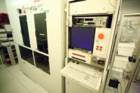
Equipment
| Lab and Coral Name | ICL / i-stepper |
| Model | Nikon NSR-2005i9 i-line(365nm) |
| Specialist | Paul Tierney (Scott Poesse) |
| Physical Location | 2F 3-North Photo |
Classification
| Process Category | Photo |
| Subcategory | Expose |
| Material Keywords | Polyimide, Other Polymers, Photoresist |
| Sample Size | 6" Wafers, 4" Wafers, Pieces Require Puck |
| Alternative | EBL / Elionix, TRL / EV-1, TRL / MA-6 |
| Keywords | multi wafer, load lock, top side of sample, alignment, requires flat |
Description
The i-stepper is a wafer level machine that exposes wafers with high resolution and great alignment, using i-line UV illumination (365nm). The stepper uses UV illumination to expose mask patterns in a photosensitive film that coats the wafer. The image that is printed is a 5x reduction of the mask (reticle) design and can be aligned to an existing wafer pattern and stepped over the entire wafer.
| Best for | Exposing high-resolution repetitive patterns at the wafer level. |
| Limitations | Sample sizes smaller than 6" wafers need to be mounted on a 6" carrier wafer which could lead to surface leveling issues and misalingment. |
| Characteristics/FOM | 50 nm alignment accuracy, 0.5 um minimum feature size |
| Caution with | Make sure you print the specifc patterns required for alingment during the first photolithography step. |
| Machine Charges | 6/wafer |
Documents
SOP
| Stepper | SOP for the Nikon i-line stepper |
| Resist Recipes | Baseline resist recipes for TRL |
| LSA Marks | How to design stepper alignment marks |
| WGA Marks | How to design stepper alignment marks |
| WGA LGA Marks | How to design stepper alignment marks |
External Links
| Guide | MicroChem Application Notes |
Process Matrix Details
Permitted
Been in the ALDSamples that have been in any of the ALD systems
, Germanium on surfaceSamples with germanium on the surface (typically grown films)
, Germanium buriedSamples with germanium buried below a different film
, PiecesWafer pieces may not be handled by the equipment, and are harder to thoroughly clean - preventing them from running in certain tools.
, Any exposure to CMOS metalIf the sample had ever seen a CMOS metal (or a tool that accepts CMOS metal), then some frontend tools could be contaminated by this.
, CMOS metal on surfaceCMOS compatible metals exposed on the surface. These are Al,Ni,Pt,Ti,TiN. Other metals such as Au are *NOT* part of this.
, CMOS metal buriedCMOS compatible metals covered entirely by a different material. These are Al,Ni,Pt,Ti,TiN. Other metals such as Au are *NOT* part of this.
, Been in the STS DRIEThe DRIE etch leaves behind polymer residues on the sidewall ripples, which can be a contamination concern for some tools.
, Been in the SEMA sample viewed in the SEM must have used the appropriate chuck to avoid cross-contamination
, Been in the Concept1The Concep1 deposits dielectrics on GREEN wafers, however it also accepts metal and there can be cross-contamination for diffusion area
, Has PhotoresistSamples with photoresist cannot be exposed to high temperatures, which is typical in deposition tools. Outgassing can be a concern.
, Has PolyimidePolyimide is a very chemically resistant polymer, and can tolerate higher temperatures but cannot be exposed to typical PECVD deposition temperatures or diffusion furnaces. Outgassing can be a concern.
, Coming from KOHAfter a KOH etch, the samples must receive a special clean because the K ions are highly contaminating to CMOS frontend tools
, Coming from CMPAfter a CMP, the samples must receive a special clean, because the slurry residues otherwise introduce contamination and particles.
Not Allowed
Ever been in EMLSamples from EML are never permitted to return to ICL or TRL
, Pyrex SubstratesPyrex substrates can be a concern due to high sodium content, which contaminates CMOS frontend tools
, III-V SubstratesAny III-V substrates, e.g. GaAs, GaN, InP, and so on. Note though that many common III-V substrates will also carry the Au flag, but there are some GREEN III-V substrates.
, Gold or RED color codeRED color code substrates. These are gold-contaminated or have been processed in gold contaminated tools. Gold and other metals can contaminate silicon devices (GREEN color code) and have to be separated.
, Has Cured SU8Not fully cured SU8 residues can heavily contaminated plasma chambers or destroy other user's samples, but fully cured SU8 is permitted in certain tools.
For more details or help, please consult PTC matrix, email ptc@mtl.mit.edu, or ask the research specialist (Paul Tierney)