Equipment
| Lab and Coral Name | EBL / Elionix |
| Model | Elionix FLS-125 |
| Specialist | Mark Mondol (Paul Tierney) |
| Physical Location | 24-041 |
Classification
| Process Category | Photo |
| Subcategory | Expose |
| Material Keywords | EBL Resist |
| Sample Size | 8" Wafers, 6" Wafers, 4" Wafers, 7" Photo Plates, 5" Photo Plates, Pieces |
| Alternative | ICL / i-stepper, TRL / MLA-150 |
| Keywords | single wafer, manual load, multiple pieces, load lock, top side of sample, vacuum, manual operation, alignment |
Description
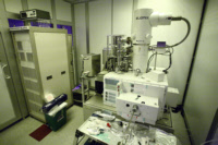
The Elionix is an electron beam lithography tool, capable of exposing e-beam resist with nanometer feature sizes. Lithography is done by scanning an electron beam over the sample according to an input file, and does not use photomasks. The exposure time is proportional to the pattern area, making the tool ideal for fine features and small total areas. Exposure doses will differ by resist types. The Layout Beamer software package can help convert designs, perform pattern logic operations, and contains the option for proximity correction. Addtionally, the software used for exposure will provide an estimate of the required write time.
| Best for | Submicron features and accurate submicron alignment of multiple layers. |
| Limitations | Large exposure areas (e.g. alignment labels, probe contact pads) can be slow to write and other lithography options such as the MLA-150 will be a faster and better choice for those. |
| Characteristics/FOM | 125 keV, current ranges from pA to 100 nA, field sizes up to 600 um |
| Caution with | Resist charging, field stitching errors, proximity effects |
| Machine Charges | 13/hour |
Documents
Process Matrix Details
Permitted
Been in the ALDSamples that have been in any of the ALD systems
, Pyrex SubstratesPyrex substrates can be a concern due to high sodium content, which contaminates CMOS frontend tools
, III-V SubstratesAny III-V substrates, e.g. GaAs, GaN, InP, and so on. Note though that many common III-V substrates will also carry the Au flag, but there are some GREEN III-V substrates.
, Germanium on surfaceSamples with germanium on the surface (typically grown films)
, Germanium buriedSamples with germanium buried below a different film
, PiecesWafer pieces may not be handled by the equipment, and are harder to thoroughly clean - preventing them from running in certain tools.
, Gold or RED color codeRED color code substrates. These are gold-contaminated or have been processed in gold contaminated tools. Gold and other metals can contaminate silicon devices (GREEN color code) and have to be separated.
, Any exposure to CMOS metalIf the sample had ever seen a CMOS metal (or a tool that accepts CMOS metal), then some frontend tools could be contaminated by this.
, CMOS metal on surfaceCMOS compatible metals exposed on the surface. These are Al,Ni,Pt,Ti,TiN. Other metals such as Au are *NOT* part of this.
, CMOS metal buriedCMOS compatible metals covered entirely by a different material. These are Al,Ni,Pt,Ti,TiN. Other metals such as Au are *NOT* part of this.
, Been in the STS DRIEThe DRIE etch leaves behind polymer residues on the sidewall ripples, which can be a contamination concern for some tools.
, Been in the SEMA sample viewed in the SEM must have used the appropriate chuck to avoid cross-contamination
(Adds), Been in the Concept1The Concep1 deposits dielectrics on GREEN wafers, however it also accepts metal and there can be cross-contamination for diffusion area
, Has PhotoresistSamples with photoresist cannot be exposed to high temperatures, which is typical in deposition tools. Outgassing can be a concern.
, Coming from KOHAfter a KOH etch, the samples must receive a special clean because the K ions are highly contaminating to CMOS frontend tools
, Coming from CMPAfter a CMP, the samples must receive a special clean, because the slurry residues otherwise introduce contamination and particles.
Not Allowed
Ever been in EMLSamples from EML are never permitted to return to ICL or TRL
, Has PolyimidePolyimide is a very chemically resistant polymer, and can tolerate higher temperatures but cannot be exposed to typical PECVD deposition temperatures or diffusion furnaces. Outgassing can be a concern.
, Has Cured SU8Not fully cured SU8 residues can heavily contaminated plasma chambers or destroy other user's samples, but fully cured SU8 is permitted in certain tools.
For more details or help, please consult PTC matrix, email ptc@mtl.mit.edu, or ask the research specialist (Mark Mondol)