Equipment
| Lab and Coral Name | TRL / MLA-150 |
| Model | Heidelberg MLA 150 |
| Specialist | Dennis Ward (Kristofor Payer) |
| Physical Location | 4F Photo-South |
Classification
| Process Category | Photo |
| Subcategory | Expose |
| Material Keywords | Photoresist |
| Sample Size | 8" Wafers, 6" Wafers, 4" Wafers, 7" Photo Plates, 5" Photo Plates, Pieces |
| Alternative | TRL / EV1, TRL / Heidelberg, ICL / i-stepper |
| Keywords | single wafer, manual load, top side of sample, manual operation, alignment |
Description
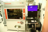
The MLA 150 is a direct-write laser system that can expose UV sensitive photoresist on wafers or masks, with the choice of a 375nm or 405 nm diode laser. Unlike the contact aligners (EV1, MA-6, EV-LC), it does not use photomasks. Exposing photoresist is the primary use of this tool. The tool is similar to the Heidelberg, but uses a DLP generate the exposure pattern, has better software, and can expose significantly faster. A full 6" wafer takes 25-45 minutes depending on the dose. A number of resist recipes exist with recommended doses. Liftoff resist (AZ5214E) needs the lowest dose (around 10 to 18 mJ/cm2), then SPR700 (around 80 mJ/cm2), and finally AZ4620 (around 200 mJ/cm2 depending on thickness). The 405nm laser has more power, and results in higher write speeds (very useful for AZ4620), which should make it the default wavelength to use. The 375nm laser is needed for certain resists. Feature sizes of 1.5um can very easily be achieved, and features can be as small as 1um or slightly less can be possible with dose optimization. A key benefit is layer-to-layer alignment, which (unlike for contact lithography), can achive alignment accuracies of 0.3 to 0.5um. Alignment can be automatic (e.g. a cross with 5-10 um line width) or manual.
| Best for | This should be the standard exposure tool for most applications. Lithography with 1um or larger feature sizes. Use 405nm laser for better write speed. Good alignment accuracy. |
| Limitations | Samples must be >5mm due to the tool's autofocus mechanism. Wafers need to be flat. Excessive bow will cause vacuum issues and prevents edge finding. The vacuum port is an X shaped trench. In MEMS devices, DRIE etched backside features may cause vacuum leaking. Ask the staff for solutions in these special cases. |
| Characteristics/FOM | 1um feature sizes, 0.3-0.5um alignment accuracy. 375nm and 405nm UV exposure. |
| Caution with | Make sure write-head is above wafer/piece before focusing, otherwise the writehead and your sample can get damaged, if the autofocus misses the sample and starts scanning the stage. |
| Machine Charges | 14/hour |
Documents
SOP
| SOP MLA-150 Load | SOP MLA-150 Loading a substrate |
| SOP MLA-150 Expose | SOP MLA-150 Exposing a substrate |
| Resist Recipes | Baseline resist recipes for TRL |
External Links
| Guide | MicroChem Application Notes |
Process Matrix Details
Permitted
Been in the ALDSamples that have been in any of the ALD systems
, Pyrex SubstratesPyrex substrates can be a concern due to high sodium content, which contaminates CMOS frontend tools
, III-V SubstratesAny III-V substrates, e.g. GaAs, GaN, InP, and so on. Note though that many common III-V substrates will also carry the Au flag, but there are some GREEN III-V substrates.
, Germanium on surfaceSamples with germanium on the surface (typically grown films)
, Germanium buriedSamples with germanium buried below a different film
, PiecesWafer pieces may not be handled by the equipment, and are harder to thoroughly clean - preventing them from running in certain tools.
, Gold or RED color codeRED color code substrates. These are gold-contaminated or have been processed in gold contaminated tools. Gold and other metals can contaminate silicon devices (GREEN color code) and have to be separated.
, Any exposure to CMOS metalIf the sample had ever seen a CMOS metal (or a tool that accepts CMOS metal), then some frontend tools could be contaminated by this.
, CMOS metal on surfaceCMOS compatible metals exposed on the surface. These are Al,Ni,Pt,Ti,TiN. Other metals such as Au are *NOT* part of this.
, CMOS metal buriedCMOS compatible metals covered entirely by a different material. These are Al,Ni,Pt,Ti,TiN. Other metals such as Au are *NOT* part of this.
, Been in the STS DRIEThe DRIE etch leaves behind polymer residues on the sidewall ripples, which can be a contamination concern for some tools.
, Been in the SEMA sample viewed in the SEM must have used the appropriate chuck to avoid cross-contamination
, Been in the Concept1The Concep1 deposits dielectrics on GREEN wafers, however it also accepts metal and there can be cross-contamination for diffusion area
, Has PhotoresistSamples with photoresist cannot be exposed to high temperatures, which is typical in deposition tools. Outgassing can be a concern.
, Has PolyimidePolyimide is a very chemically resistant polymer, and can tolerate higher temperatures but cannot be exposed to typical PECVD deposition temperatures or diffusion furnaces. Outgassing can be a concern.
, Has Cured SU8Not fully cured SU8 residues can heavily contaminated plasma chambers or destroy other user's samples, but fully cured SU8 is permitted in certain tools.
, Coming from KOHAfter a KOH etch, the samples must receive a special clean because the K ions are highly contaminating to CMOS frontend tools
, Coming from CMPAfter a CMP, the samples must receive a special clean, because the slurry residues otherwise introduce contamination and particles.
Not Allowed
Ever been in EMLSamples from EML are never permitted to return to ICL or TRL
For more details or help, please consult PTC matrix, email ptc@mtl.mit.edu, or ask the research specialist (Dennis Ward )