Equipment
| Lab and Coral Name | TRL / HMDS-TRL |
| Model | Yes |
| Specialist | David Terry (Dennis Ward) |
| Physical Location | 4F Photo-North |
Classification
| Process Category | Photo |
| Subcategory | Bake |
| Material Keywords | Silicon, SiO2, SiNx |
| Sample Size | 6" Wafers, 4" Wafers, Pieces |
| Alternative | TRL / postbake |
| Keywords | multi wafer, manual load, multiple pieces, both sides of sample, conformal dep, vacuum, temperature |
Description
The HMDS-TRL is a vacuum oven that is used in preparing samples for PR coating. It dehydrates the samples and applies HMDS as an adhesion promoter. The oven cycles through several pump-purge cycles, dehydrating the sample and evacuating the chamber, then applies HMDS vapor to coat the sample, followed by additonal pump-purge cycles. The overall run takes around 15-20 minutes. Some surfaces (e.g. metals) may not directly benefit from the HMDS application, but the pump-purge cycles can nonetheless be useful for dehydrating the samples. Similar dehydration may be achieved using the hotplate1 or similar hotplates. Different HMDS programs exist depending on the resist type (thin vs thick), as detailed in the SOP and on the tool itself.
| Best for | Dehydration and HMDS application before PR coating |
| Limitations | Organic materials are not allowed in the oven. HMDS may not be necessary for certain substrates (e.g. metals). |
| Characteristics/FOM | batch, manual load, 150C temperature |
| Caution with | The metal boat and wafers will be at 150C temperature, so let them cool down on glass surface at coater before spinning PR. Do not transfer onto fabwipes or into box immediately, because at that temperature the wipes or box will melt. Use tongs or handles to avoid accidental burns. |
| Machine Charges | no charge |
Documents
SOP
| Resist Recipes | Baseline resist recipes for TRL |
Documents
| HMDS Oven | Application Note describing HMDS procedures |
Images
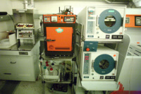
| HMDS Oven | 1: Photo of the HMDS oven in TRL |
External Links
| Guide | MicroChem Application Notes |
Process Matrix Details
Permitted
Been in the ALDSamples that have been in any of the ALD systems
, Pyrex SubstratesPyrex substrates can be a concern due to high sodium content, which contaminates CMOS frontend tools
, III-V SubstratesAny III-V substrates, e.g. GaAs, GaN, InP, and so on. Note though that many common III-V substrates will also carry the Au flag, but there are some GREEN III-V substrates.
, Germanium on surfaceSamples with germanium on the surface (typically grown films)
, Germanium buriedSamples with germanium buried below a different film
, PiecesWafer pieces may not be handled by the equipment, and are harder to thoroughly clean - preventing them from running in certain tools.
, Gold or RED color codeRED color code substrates. These are gold-contaminated or have been processed in gold contaminated tools. Gold and other metals can contaminate silicon devices (GREEN color code) and have to be separated.
, Any exposure to CMOS metalIf the sample had ever seen a CMOS metal (or a tool that accepts CMOS metal), then some frontend tools could be contaminated by this.
, CMOS metal on surfaceCMOS compatible metals exposed on the surface. These are Al,Ni,Pt,Ti,TiN. Other metals such as Au are *NOT* part of this.
, CMOS metal buriedCMOS compatible metals covered entirely by a different material. These are Al,Ni,Pt,Ti,TiN. Other metals such as Au are *NOT* part of this.
, Been in the STS DRIEThe DRIE etch leaves behind polymer residues on the sidewall ripples, which can be a contamination concern for some tools.
, Been in the SEMA sample viewed in the SEM must have used the appropriate chuck to avoid cross-contamination
, Been in the Concept1The Concep1 deposits dielectrics on GREEN wafers, however it also accepts metal and there can be cross-contamination for diffusion area
, Has PhotoresistSamples with photoresist cannot be exposed to high temperatures, which is typical in deposition tools. Outgassing can be a concern.
, Has PolyimidePolyimide is a very chemically resistant polymer, and can tolerate higher temperatures but cannot be exposed to typical PECVD deposition temperatures or diffusion furnaces. Outgassing can be a concern.
, Has Cured SU8Not fully cured SU8 residues can heavily contaminated plasma chambers or destroy other user's samples, but fully cured SU8 is permitted in certain tools.
, Coming from KOHAfter a KOH etch, the samples must receive a special clean because the K ions are highly contaminating to CMOS frontend tools
, Coming from CMPAfter a CMP, the samples must receive a special clean, because the slurry residues otherwise introduce contamination and particles.
Not Allowed
Ever been in EMLSamples from EML are never permitted to return to ICL or TRL
For more details or help, please consult PTC matrix, email ptc@mtl.mit.edu, or ask the research specialist (David Terry)