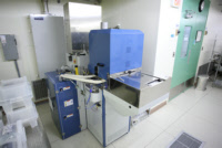
Equipment
| Lab and Coral Name | ICL / ALD-Oxford |
| Model | Oxford FlexAl |
| Specialist | Donal Jamieson (Paudely Zamora) |
| Physical Location | 2F 1-South Metrology |
Classification
| Process Category | Deposition |
| Subcategory | CVD, PECVD |
| Material Keywords | Dielectrics, CMOS Metals, Non-Standard Materials |
| Sample Size | 6" Wafers, 4" Wafers, Pieces |
| Alternative | ICL / ALD |
| Keywords | single wafer, multiple pieces, load lock, top side of sample, conformal dep, vacuum, plasma, temperature |
Description
The ALD-Oxford is a atomic layer deposition tool that can deposit Al2O3, AlN, HfO2 and TiN. It can deposit layers both by plasma- and thermal-assisted processing. Films of <5 nm thicknesses can be deposited with good uniformity and at relatively low temperatures. Deposition can be done on materials such as Si and "GREEN" III-N samples. Proper cleaning procedures (RCA or PIRHANA) are required on samples before deposition, to maintain a high level of cleanliness in the system. No metals are allowed in the tool.
| Best for | Deposition of gate dielectric layers, conformal and uniform deposition for <5 nm layers. |
| Limitations | Slow deposition rate, relatively thin layers. |
| Characteristics/FOM | Plasma or thermal assisted ALD deposition. |
| Caution with | Sample cleaning is required (RCA or PIRAHNA). Photoresist (or any polymer) and metals are not allowed in this tool. |
| Machine Charges | 7/wafer + 120/um |
Documents
SOP
| Oxford ALD | SOP for the Oxford ALD |
Process Matrix Details
Permitted
Been in the ALDSamples that have been in any of the ALD systems
(Adds), III-V SubstratesAny III-V substrates, e.g. GaAs, GaN, InP, and so on. Note though that many common III-V substrates will also carry the Au flag, but there are some GREEN III-V substrates.
, Germanium on surfaceSamples with germanium on the surface (typically grown films)
, Germanium buriedSamples with germanium buried below a different film
, PiecesWafer pieces may not be handled by the equipment, and are harder to thoroughly clean - preventing them from running in certain tools.
, Any exposure to CMOS metalIf the sample had ever seen a CMOS metal (or a tool that accepts CMOS metal), then some frontend tools could be contaminated by this.
, CMOS metal on surfaceCMOS compatible metals exposed on the surface. These are Al,Ni,Pt,Ti,TiN. Other metals such as Au are *NOT* part of this.
, CMOS metal buriedCMOS compatible metals covered entirely by a different material. These are Al,Ni,Pt,Ti,TiN. Other metals such as Au are *NOT* part of this.
, Been in the SEMA sample viewed in the SEM must have used the appropriate chuck to avoid cross-contamination
, Been in the Concept1The Concep1 deposits dielectrics on GREEN wafers, however it also accepts metal and there can be cross-contamination for diffusion area
, Coming from KOHAfter a KOH etch, the samples must receive a special clean because the K ions are highly contaminating to CMOS frontend tools
, Coming from CMPAfter a CMP, the samples must receive a special clean, because the slurry residues otherwise introduce contamination and particles.
Not Allowed
Ever been in EMLSamples from EML are never permitted to return to ICL or TRL
, Pyrex SubstratesPyrex substrates can be a concern due to high sodium content, which contaminates CMOS frontend tools
, Gold or RED color codeRED color code substrates. These are gold-contaminated or have been processed in gold contaminated tools. Gold and other metals can contaminate silicon devices (GREEN color code) and have to be separated.
, Been in the STS DRIEThe DRIE etch leaves behind polymer residues on the sidewall ripples, which can be a contamination concern for some tools.
, Has PhotoresistSamples with photoresist cannot be exposed to high temperatures, which is typical in deposition tools. Outgassing can be a concern.
, Has PolyimidePolyimide is a very chemically resistant polymer, and can tolerate higher temperatures but cannot be exposed to typical PECVD deposition temperatures or diffusion furnaces. Outgassing can be a concern.
, Has Cured SU8Not fully cured SU8 residues can heavily contaminated plasma chambers or destroy other user's samples, but fully cured SU8 is permitted in certain tools.
, Has been past RCA clean for over 4 hoursFor some diffusion furnaces, the samples must immideatly enter the furnace and cannot be stored in a box for a long time.
For more details or help, please consult PTC matrix, email ptc@mtl.mit.edu, or ask the research specialist (Donal Jamieson)