Equipment
| Lab and Coral Name | ICL / ALD |
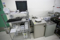
| Model | Thermolyne Furnace, 6000 |
| Specialist | Donal Jamieson (Paudely Zamora) |
| Physical Location | 2F 1-North Deposition |
Classification
| Process Category | Deposition |
| Subcategory | CVD |
| Material Keywords | Dielectrics, CMOS Metals, Non-Standard Materials |
| Sample Size | 6" Wafers, 4" Wafers, Pieces |
| Alternative | ICL / ALD-Oxford |
| Keywords | single wafer, manual load, multiple pieces, top side of sample, conformal dep, vacuum, temperature, manual operation |
Description
The ALD is an atomic layer deposition tool for Al2O3, HfO2 and WN. It deposits thin films by thermal-assisted processing, for RED processes. The deposition takes place in an atomic layer-by-layer fashion, and thereby allows for atomic-scale control of the film thickness. Thin layers (sub-5 nm) are deposited with extremly good uniformity and conformal coverage, and at relatively low temperatures (typically below 300 C). Films can be deposited onto Si, III-V and 2D materials. Proper cleaning of the samples (e.g. RCA, Piranha, nanostrip, O2 plasma, etc) before deposition is required to help maintain the cleanliness of the system. No organics (e.g. photoresists) are allowed in this tool.
| Best for | Gate dielectric layers, very thin films, conformal coverage, uniform deposition for sub-5nm layers. |
| Limitations | Slow deposition rate, relatively thin layers only |
| Characteristics/FOM | Al2O3, HfO2, WN |
| Caution with | Proper sample cleaning is required (the choice of cleaning procedures can vary by samples type depending on what it is able to tolerate), to maintain the cleanliness of the tool, since it is critical to a number of applications. No organics (polymers, photoresists, etc) are allowed. |
| Machine Charges | 7/wafer + 120/um |
Documents
SOP
| ALD | SOP for the Cambridge Nano ALD |
Process Matrix Details
Permitted
Been in the ALDSamples that have been in any of the ALD systems
(Adds), III-V SubstratesAny III-V substrates, e.g. GaAs, GaN, InP, and so on. Note though that many common III-V substrates will also carry the Au flag, but there are some GREEN III-V substrates.
, Germanium on surfaceSamples with germanium on the surface (typically grown films)
, Germanium buriedSamples with germanium buried below a different film
, PiecesWafer pieces may not be handled by the equipment, and are harder to thoroughly clean - preventing them from running in certain tools.
, Gold or RED color codeRED color code substrates. These are gold-contaminated or have been processed in gold contaminated tools. Gold and other metals can contaminate silicon devices (GREEN color code) and have to be separated.
, Any exposure to CMOS metalIf the sample had ever seen a CMOS metal (or a tool that accepts CMOS metal), then some frontend tools could be contaminated by this.
, CMOS metal on surfaceCMOS compatible metals exposed on the surface. These are Al,Ni,Pt,Ti,TiN. Other metals such as Au are *NOT* part of this.
, CMOS metal buriedCMOS compatible metals covered entirely by a different material. These are Al,Ni,Pt,Ti,TiN. Other metals such as Au are *NOT* part of this.
, Been in the SEMA sample viewed in the SEM must have used the appropriate chuck to avoid cross-contamination
, Been in the Concept1The Concep1 deposits dielectrics on GREEN wafers, however it also accepts metal and there can be cross-contamination for diffusion area
, Coming from KOHAfter a KOH etch, the samples must receive a special clean because the K ions are highly contaminating to CMOS frontend tools
, Coming from CMPAfter a CMP, the samples must receive a special clean, because the slurry residues otherwise introduce contamination and particles.
Not Allowed
Ever been in EMLSamples from EML are never permitted to return to ICL or TRL
, Pyrex SubstratesPyrex substrates can be a concern due to high sodium content, which contaminates CMOS frontend tools
, Been in the STS DRIEThe DRIE etch leaves behind polymer residues on the sidewall ripples, which can be a contamination concern for some tools.
, Has PhotoresistSamples with photoresist cannot be exposed to high temperatures, which is typical in deposition tools. Outgassing can be a concern.
, Has PolyimidePolyimide is a very chemically resistant polymer, and can tolerate higher temperatures but cannot be exposed to typical PECVD deposition temperatures or diffusion furnaces. Outgassing can be a concern.
, Has Cured SU8Not fully cured SU8 residues can heavily contaminated plasma chambers or destroy other user's samples, but fully cured SU8 is permitted in certain tools.
, Has been past RCA clean for over 4 hoursFor some diffusion furnaces, the samples must immideatly enter the furnace and cannot be stored in a box for a long time.
For more details or help, please consult PTC matrix, email ptc@mtl.mit.edu, or ask the research specialist (Donal Jamieson)