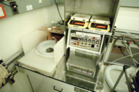
Equipment
| Lab and Coral Name | TRL / coater |
| Model | Solitec 5110 |
| Specialist | David Terry (Paul Tierney) |
| Physical Location | 4F Photo-North |
Classification
| Process Category | Photo |
| Subcategory | Coat |
| Material Keywords | Polyimide, Other Polymers, Photoresist, EBL Resist |
| Sample Size | 6" Wafers, 4" Wafers, Pieces |
| Alternative | TRL / PMMAspinner |
| Keywords | single wafer, manual load, top side of sample, conformal dep, manual operation, spinning substrate |
Description
The coater is a multi-stage spinner that can be programmed with separate speed/time settings for dispense, spread, and spin. Auto-dispense of resist is available for SPR700-1.0, AZ5214E, AZ4620. The coating is done one piece or one wafer at a time.
| Best for | PR coating (built-in SPR700, AZ5214E, AZ4620). Different chucks for wafers and pieces. |
| Limitations | One sample at a time with manual loading. |
| Characteristics/FOM | SPR700, AZ5214E, AZ4620. User-supplied PTC approved resists. |
| Caution with | Mount corresponding chuck for RED and GREEN processes. Keep hands off while spinning. Fragile wafers can fly off chuck and break if vacuum not good. |
| Machine Charges | 2/wafer |
Documents
SOP
| Resist Recipes | Baseline resist recipes for TRL |
| Target-Mounting | How to handle-mount wafers for the sts1 and sts2 |
Documents
| AZ5214E | Datasheet for AZ5214E image reversal resist |
| AZ4620 | Datasheet for AZ4620 thick resist |
| Photoresist | Application Note describing photoresist chemistry |
| Liftoff Resist | Application Note describing liftoff resists |
| Image reversal | Application Note describing image reversal |
| Coating | Application Note describing spincoating |
| Developing Resist | Application Note describing resist development |
| PI Selection | Application Note describing polyimide choices |
| HD4100 | Datasheet for HD4100 polyimide |
| maN2400 | Datasheet for maN2400 e-beam resist |
External Links
| Guide | MicroChem Application Notes |
Process Matrix Details
Permitted
Been in the ALDSamples that have been in any of the ALD systems
, Pyrex SubstratesPyrex substrates can be a concern due to high sodium content, which contaminates CMOS frontend tools
, III-V SubstratesAny III-V substrates, e.g. GaAs, GaN, InP, and so on. Note though that many common III-V substrates will also carry the Au flag, but there are some GREEN III-V substrates.
, Germanium on surfaceSamples with germanium on the surface (typically grown films)
, Germanium buriedSamples with germanium buried below a different film
, PiecesWafer pieces may not be handled by the equipment, and are harder to thoroughly clean - preventing them from running in certain tools.
, Gold or RED color codeRED color code substrates. These are gold-contaminated or have been processed in gold contaminated tools. Gold and other metals can contaminate silicon devices (GREEN color code) and have to be separated.
, Any exposure to CMOS metalIf the sample had ever seen a CMOS metal (or a tool that accepts CMOS metal), then some frontend tools could be contaminated by this.
, CMOS metal on surfaceCMOS compatible metals exposed on the surface. These are Al,Ni,Pt,Ti,TiN. Other metals such as Au are *NOT* part of this.
, CMOS metal buriedCMOS compatible metals covered entirely by a different material. These are Al,Ni,Pt,Ti,TiN. Other metals such as Au are *NOT* part of this.
, Been in the STS DRIEThe DRIE etch leaves behind polymer residues on the sidewall ripples, which can be a contamination concern for some tools.
, Been in the SEMA sample viewed in the SEM must have used the appropriate chuck to avoid cross-contamination
, Been in the Concept1The Concep1 deposits dielectrics on GREEN wafers, however it also accepts metal and there can be cross-contamination for diffusion area
, Has PhotoresistSamples with photoresist cannot be exposed to high temperatures, which is typical in deposition tools. Outgassing can be a concern.
, Has PolyimidePolyimide is a very chemically resistant polymer, and can tolerate higher temperatures but cannot be exposed to typical PECVD deposition temperatures or diffusion furnaces. Outgassing can be a concern.
, Coming from KOHAfter a KOH etch, the samples must receive a special clean because the K ions are highly contaminating to CMOS frontend tools
, Coming from CMPAfter a CMP, the samples must receive a special clean, because the slurry residues otherwise introduce contamination and particles.
Not Allowed
Ever been in EMLSamples from EML are never permitted to return to ICL or TRL
, Has Cured SU8Not fully cured SU8 residues can heavily contaminated plasma chambers or destroy other user's samples, but fully cured SU8 is permitted in certain tools.
For more details or help, please consult PTC matrix, email ptc@mtl.mit.edu, or ask the research specialist (David Terry)