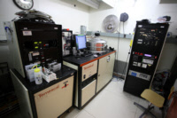
Equipment
| Lab and Coral Name | TRL / eBeamAu |
| Model | Temescal VES2550 |
| Specialist | David Terry (Paudely Zamora) |
| Physical Location | 4F Deposition |
Classification
| Process Category | Deposition |
| Subcategory | Evaporate |
| Material Keywords | Dielectrics, CMOS Metals, Non-CMOS Metals, Non-Standard Materials, Photoresist, EBL Resist |
| Sample Size | 6" Wafers, 4" Wafers, Pieces |
| Alternative | TRL / eBeamFP |
| Keywords | multi wafer, manual load, multiple pieces, top side of sample, directional dep, vacuum, manual operation |
Description
The eBeamAu is a metal evaporator that uses an electron beam to heat a target under ultra-high vacuum. The electron beam that heats the target material sweeps in a pattern to create a small melted area of material. The target atoms then evaporate and precipitate into solid form onto the sample. Without a good vacuum, film quality suffers as the direct path to the substrate is interrupted. Occasionally, outgassing of the target can cause the vaccum to dump and the deposition to be aborted, in which case the recipe can be re-run with adjusted thickness. The deposited film is measured with a crystal. Power levels and ramp-up condition for the electron beam as well as crystal parameters are highly specific to the material deposited. Plates for 6" and 4" wafers exist, and allow many wafers to be processed at the same time. Smaller samples can be attaced to appropriate clip-holders. Zero rotation can be used for liftoff on pieces, if the clip holder is placed on the horizontal plate, and positioned properly. Interchangeable targets (up to 4 per run), user supplied targets are possible if allowed with staff and PTC approval.
| Best for | Depositing metal patterns through liftoff, broadest range of materials for deposition |
| Limitations | Pump-down time can be as long as 90 minutes. Switching between materials requires cooldown. Maximum reservation time is 4 hours, if longer needed, please contact staff. |
| Characteristics/FOM | Four crucibles can deposit up to four different materials during the run (in any order). |
| Caution with | Caution when loading and unloading of crucibles to avoid jamming the holder. Always inspect crucible fill height at the beginning and during deposition. If deposition rate is atypical, inspect crucible through viewport, and abort process to seek help from staff. Depositing from an empty or damaged crucible can result in severe tool damage. |
| Machine Charges | 20/run + 80/um** |
Documents
SOP
| Metal Evaporator | SOP for the e-beam evaporator |
Process Matrix Details
Permitted
Been in the ALDSamples that have been in any of the ALD systems
, Pyrex SubstratesPyrex substrates can be a concern due to high sodium content, which contaminates CMOS frontend tools
, III-V SubstratesAny III-V substrates, e.g. GaAs, GaN, InP, and so on. Note though that many common III-V substrates will also carry the Au flag, but there are some GREEN III-V substrates.
, Germanium on surfaceSamples with germanium on the surface (typically grown films)
, Germanium buriedSamples with germanium buried below a different film
, PiecesWafer pieces may not be handled by the equipment, and are harder to thoroughly clean - preventing them from running in certain tools.
, Gold or RED color codeRED color code substrates. These are gold-contaminated or have been processed in gold contaminated tools. Gold and other metals can contaminate silicon devices (GREEN color code) and have to be separated.
(Adds), Any exposure to CMOS metalIf the sample had ever seen a CMOS metal (or a tool that accepts CMOS metal), then some frontend tools could be contaminated by this.
(Adds), CMOS metal on surfaceCMOS compatible metals exposed on the surface. These are Al,Ni,Pt,Ti,TiN. Other metals such as Au are *NOT* part of this.
(Adds), CMOS metal buriedCMOS compatible metals covered entirely by a different material. These are Al,Ni,Pt,Ti,TiN. Other metals such as Au are *NOT* part of this.
, Been in the STS DRIEThe DRIE etch leaves behind polymer residues on the sidewall ripples, which can be a contamination concern for some tools.
, Been in the SEMA sample viewed in the SEM must have used the appropriate chuck to avoid cross-contamination
, Been in the Concept1The Concep1 deposits dielectrics on GREEN wafers, however it also accepts metal and there can be cross-contamination for diffusion area
, Has PhotoresistSamples with photoresist cannot be exposed to high temperatures, which is typical in deposition tools. Outgassing can be a concern.
, Has PolyimidePolyimide is a very chemically resistant polymer, and can tolerate higher temperatures but cannot be exposed to typical PECVD deposition temperatures or diffusion furnaces. Outgassing can be a concern.
, Has Cured SU8Not fully cured SU8 residues can heavily contaminated plasma chambers or destroy other user's samples, but fully cured SU8 is permitted in certain tools.
, Coming from KOHAfter a KOH etch, the samples must receive a special clean because the K ions are highly contaminating to CMOS frontend tools
, Coming from CMPAfter a CMP, the samples must receive a special clean, because the slurry residues otherwise introduce contamination and particles.
Not Allowed
Ever been in EMLSamples from EML are never permitted to return to ICL or TRL
For more details or help, please consult PTC matrix, email ptc@mtl.mit.edu, or ask the research specialist (David Terry)