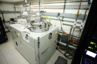
Equipment
| Lab and Coral Name | TRL / eBeamFP |
| Model | Temescal FC2000 |
| Specialist | Paudely Zamora (Timothy Turner) |
| Physical Location | 4F External-Deposition |
Classification
| Process Category | Deposition |
| Subcategory | Evaporate |
| Material Keywords | CMOS Metals, Non-CMOS Metals, Photoresist, EBL Resist |
| Sample Size | 6" Wafers, 4" Wafers, Pieces |
| Alternative | TRL / eBeamAu |
| Keywords | multi wafer, manual load, multiple pieces, load lock, top side of sample, directional dep, vacuum |
Description
The eBeamFP is a metal evaporator that uses an electron beam to heat a target under ultra-high vacuum. The electron beam that heats the target material sweeps in a pattern to create a small melted area of material. The target atoms then evaporate and precipitate into solid form onto the sample. The material choices can not be modified, but the presence of a loadlock allows for very fast pump downs (so a deposition usually takes 1 hour from load to unload). The deposited film is measured with a crystal. Power levels and ramp-up condition for the electron beam as well as crystal parameters are highly specific to the material deposited, and part of the built in recipes. Plates for 6" and 4" wafers exist, and up to five 6" wafers can be processed at the same time. Smaller samples can be attached to appropriate clip-holders. Unlike the eBeamAu, for the FP, zero rotation it not useful because the wafers are held at an angle, so that every wafer position is at equal distance from the metal source and orthogonal to the path of evaporation. However, some users use zero roation with pieces if they are concerned about their pieces falling from the clip holders when rotating.
| Best for | Patterning metals through liftoff, load lock allows for fast pumpdown (e.g. around 10-25 minutes). |
| Limitations | Target materials (Ti, Au, Pt, Al, Ni, Ge) cannot be modified. Recipes should not be modified except for deposition times. |
| Characteristics/FOM | Ti, Au, Pt, Al, Ni, Ge |
| Caution with | Always inspect crucible fill height at the beginning and during deposition. If deposition rate is atypical, inspect crucible through viewport, and abort process to seek help from staff. Depositing from an empty or damaged crucible can result in severe tool damage. |
| Machine Charges | 20/run + 80/um** |
Documents
SOP
| Metal Evaporator | SOP for the e-beam evaporator |
Process Matrix Details
Permitted
Been in the ALDSamples that have been in any of the ALD systems
, Pyrex SubstratesPyrex substrates can be a concern due to high sodium content, which contaminates CMOS frontend tools
, III-V SubstratesAny III-V substrates, e.g. GaAs, GaN, InP, and so on. Note though that many common III-V substrates will also carry the Au flag, but there are some GREEN III-V substrates.
, Germanium on surfaceSamples with germanium on the surface (typically grown films)
, Germanium buriedSamples with germanium buried below a different film
, PiecesWafer pieces may not be handled by the equipment, and are harder to thoroughly clean - preventing them from running in certain tools.
, Gold or RED color codeRED color code substrates. These are gold-contaminated or have been processed in gold contaminated tools. Gold and other metals can contaminate silicon devices (GREEN color code) and have to be separated.
(Adds), Any exposure to CMOS metalIf the sample had ever seen a CMOS metal (or a tool that accepts CMOS metal), then some frontend tools could be contaminated by this.
(Adds), CMOS metal on surfaceCMOS compatible metals exposed on the surface. These are Al,Ni,Pt,Ti,TiN. Other metals such as Au are *NOT* part of this.
(Adds), CMOS metal buriedCMOS compatible metals covered entirely by a different material. These are Al,Ni,Pt,Ti,TiN. Other metals such as Au are *NOT* part of this.
, Been in the STS DRIEThe DRIE etch leaves behind polymer residues on the sidewall ripples, which can be a contamination concern for some tools.
, Been in the SEMA sample viewed in the SEM must have used the appropriate chuck to avoid cross-contamination
, Been in the Concept1The Concep1 deposits dielectrics on GREEN wafers, however it also accepts metal and there can be cross-contamination for diffusion area
, Has PhotoresistSamples with photoresist cannot be exposed to high temperatures, which is typical in deposition tools. Outgassing can be a concern.
, Has PolyimidePolyimide is a very chemically resistant polymer, and can tolerate higher temperatures but cannot be exposed to typical PECVD deposition temperatures or diffusion furnaces. Outgassing can be a concern.
, Has Cured SU8Not fully cured SU8 residues can heavily contaminated plasma chambers or destroy other user's samples, but fully cured SU8 is permitted in certain tools.
, Coming from KOHAfter a KOH etch, the samples must receive a special clean because the K ions are highly contaminating to CMOS frontend tools
, Coming from CMPAfter a CMP, the samples must receive a special clean, because the slurry residues otherwise introduce contamination and particles.
Not Allowed
Ever been in EMLSamples from EML are never permitted to return to ICL or TRL
For more details or help, please consult PTC matrix, email ptc@mtl.mit.edu, or ask the research specialist (Paudely Zamora)