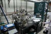
Equipment
| Lab and Coral Name | EML / SputtererAJA |
| Model | AJA Orion 5 |
| Specialist | Kurt Broderick (Timothy Turner, Gary Riggott) |
| Physical Location | 5F 2-North |
Classification
| Process Category | Deposition |
| Subcategory | Sputter |
| Material Keywords | Dielectrics, CMOS Metals, Non-CMOS Metals, Non-Standard Materials |
| Sample Size | 6" Wafers, 4" Wafers, Pieces |
| Alternative | TRL / AJA-TRL, EML / eBeam-AJA |
| Keywords | single wafer, manual load, multiple pieces, load lock, top side of sample, conformal dep, vacuum, plasma, manual operation |
Description
The sputterer in EML allows for the deposition of a wide variety of metals, dielectrics, and semiconductors. Reactive sputtering with O2 or N2 allows for the deposition of oxides and nitrides of these materials as well. Samples are manually loaded at the bottom of the chamber, face-up, on a rotating stage. Sputtering targets are can be changed by each user. Up to four separate targets can be loaded at a time. Up to two DC and two RF power sources are available. Substrate bias is available for etchback. Substrate heating is also available. Deposition runs of multiple metals is possible in series without the need for additional pumpdowns or venting, on wafers or pieces 3" or smaller.
| Best for | Conformal film deposition |
| Limitations | Deposition rate can only be measured during dummy run without a sample on the stage. |
| Characteristics/FOM | DC Deposition rate (per target) < 2 A/s, Maximum practical substrate temperature 550C |
| Caution with | |
| Machine Charges | 10/wafer + 80/um** |
Documents
SOP
| AJA Sputterer | SOP for the AJA sputterer |
Process Matrix Details
PTC Matrix does not apply for EML
Ever been in EMLSamples from EML are never permitted to return to ICL or TRL