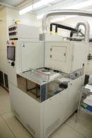
Equipment
| Lab and Coral Name | TRL / SAMCO |
| Model | SAMCO 200iP |
| Specialist | Eric Lim (Robert Bicchieri) |
| Physical Location | 4F Main-North |
Classification
| Process Category | Etch |
| Subcategory | RIE |
| Material Keywords | III-V, GaN, CMOS Metals, Non-CMOS Metals, 2D Materials |
| Sample Size | 6" Wafers, 4" Wafers, Pieces |
| Alternative | TRL / Plasmaquest |
| Keywords | single wafer, multiple pieces, load lock, top side of sample, anisotropic etch, vacuum, plasma, temperature |
Description
The SAMCO is a RED ICP-RIE that etches III-V compounds (GaAs, GaN, InP, InGaAs, GaSb, etc) using chlorine chemistries. The substrate can be heated up to 250C (e.g. to allow etching of In III-V's). The high density plasma is achieved by a separate plasma source and enables high etch rates. Low chamber pressure (< 5 mTorr) can enable vertical profiles. A hard mask is preferred over a photoresist mask, beause resist can easily burn during the etch.
| Best for | III-V (GaAs, GaN, InP, InGaAs, GaSb, etc) dry etches with high aspect-ratio profiles and smooth sidewalls |
| Limitations | Photoresist masks will degrade really quickly in the plasma and are not appropriate for long etches. Photoresist will also bubble and burn during the etch, making it very hard to remove afterwards. |
| Characteristics/FOM | ICP-RIE. Electrostatic chuck for stable sample transfer process. Gas: Cl2, BCl3, SiCl4, Ar, N2, O2 and CHF3. O2 and CHF3 are mainly used for chamber cleaning purpose and should not be used for etching. |
| Caution with | For etches that require the chuck to be at a high temperature, make sure you reserve enough time to allow for temperature stabilization and for cooldown after the etch. At the end of your reservation the chamber temperature needs to be stabilized to the default, 40C. |
| Machine Charges | 7/wafer + 1/um |
Documents
SOP
| Samco ICP Etcher | SOP for the SAMCO etcher |
Documents
| Etch rates part 2 | Berkeley etch rate paper |
| Etch rates part 1 | Berkeley etch rate paper |
External Links
| Dry Etching for VLSI | Fundamentals of dry etching, good introduction text |
Process Matrix Details
Permitted
Been in the ALDSamples that have been in any of the ALD systems
, Pyrex SubstratesPyrex substrates can be a concern due to high sodium content, which contaminates CMOS frontend tools
, III-V SubstratesAny III-V substrates, e.g. GaAs, GaN, InP, and so on. Note though that many common III-V substrates will also carry the Au flag, but there are some GREEN III-V substrates.
, Germanium on surfaceSamples with germanium on the surface (typically grown films)
, Germanium buriedSamples with germanium buried below a different film
, PiecesWafer pieces may not be handled by the equipment, and are harder to thoroughly clean - preventing them from running in certain tools.
, Gold or RED color codeRED color code substrates. These are gold-contaminated or have been processed in gold contaminated tools. Gold and other metals can contaminate silicon devices (GREEN color code) and have to be separated.
(Adds), Any exposure to CMOS metalIf the sample had ever seen a CMOS metal (or a tool that accepts CMOS metal), then some frontend tools could be contaminated by this.
(Adds), CMOS metal on surfaceCMOS compatible metals exposed on the surface. These are Al,Ni,Pt,Ti,TiN. Other metals such as Au are *NOT* part of this.
, CMOS metal buriedCMOS compatible metals covered entirely by a different material. These are Al,Ni,Pt,Ti,TiN. Other metals such as Au are *NOT* part of this.
, Been in the STS DRIEThe DRIE etch leaves behind polymer residues on the sidewall ripples, which can be a contamination concern for some tools.
, Been in the SEMA sample viewed in the SEM must have used the appropriate chuck to avoid cross-contamination
, Been in the Concept1The Concep1 deposits dielectrics on GREEN wafers, however it also accepts metal and there can be cross-contamination for diffusion area
, Has PhotoresistSamples with photoresist cannot be exposed to high temperatures, which is typical in deposition tools. Outgassing can be a concern.
, Has PolyimidePolyimide is a very chemically resistant polymer, and can tolerate higher temperatures but cannot be exposed to typical PECVD deposition temperatures or diffusion furnaces. Outgassing can be a concern.
, Has Cured SU8Not fully cured SU8 residues can heavily contaminated plasma chambers or destroy other user's samples, but fully cured SU8 is permitted in certain tools.
, Coming from KOHAfter a KOH etch, the samples must receive a special clean because the K ions are highly contaminating to CMOS frontend tools
, Coming from CMPAfter a CMP, the samples must receive a special clean, because the slurry residues otherwise introduce contamination and particles.
Not Allowed
Ever been in EMLSamples from EML are never permitted to return to ICL or TRL
For more details or help, please consult PTC matrix, email ptc@mtl.mit.edu, or ask the research specialist (Eric Lim)